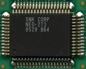
NEO-273

| |
| Package | QFP64R |
| Manufacturer | |
| First use | 1992 ? |
| Used on | MVS cartridges |
The NEO-273 chip is used in cartridges to replace discrete 74LS273 and 74LS174 latches that were used in early boards (like on CHA-32). It demultiplexes the P bus to C ROM and S ROM addresses.
This chip was later replaced by NEO-CMC which performs the same functions along with a lot of other things.
For cartridges that use this chip but have more than 8MiB of sprite graphics data, extra bits were added using discrete chips. An added 74LS74 (2 bits) in CHA256 boards for example increases the C ROM capacity from 8MiB to 32MiB (256Mbits).
Demultiplexing
- The C ROM address is latched on the rising edge of PCK1B.
- The S ROM address is latched on the rising edge of PCK2B.
See P bus.
| P BUS | P19 | P18 | P17 | P16 | P15 | P14 | P13 | P12 | P11 | P10 | P9 | P8 | P7 | P6 | P5 | P4 | P3 | P2 | P1 | P0 |
|---|---|---|---|---|---|---|---|---|---|---|---|---|---|---|---|---|---|---|---|---|
| C address | A3 | A2 | A1 | A0 | A20 | A19 | A18 | A17 | A16 | A15 | A14 | A13 | A12 | A11 | A10 | A9 | A8 | A7 | A6 | A5 |
| S address | A4 | A2 | A1 | A0 | ||||||||||||||||
P20~23 are left out or routed to additional latches.
A /C_A20 signal is available on pin 47 to allow cartridges which use 2MiB C ROMs to switch between 2 pairs without the need for an additional inverter chip.
Internals
It includes one 16-bit latch (to address a 128KiB S ROM) and one 20-bit latch (to address 8MiB of 2*16bits C ROMs).
Note that A4 (CA4) of the C ROMs and A3 (2H1) of the S ROM are not part of the P bus and come straight from the cartridge edge, bypassing this chip.
Pinout
OpenOffice Draw file: File:Neo-273.odg