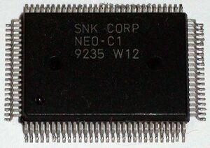
NEO-C1

Also found on MVS boards.
Handles both joypad ports inputs and drives the /OE lines for various chips (Battery-backed RAM, LSPC...)
Pinout
68k
- A17~A21: 68k address bus
- A22I~A23I: NEO-E0 address input
- D8~D15: 68k data bus
- R/W,UDS,LDS,AS,DTACK: 68k bus control signals
- 68KCLK: 12MHz 68k clock
- ROMWAIT,PWAIT0,PWAIT1,PDTACK: signals from cart PROG board to configure how /DTACK is generated for ROMOE region (how is it configured?)
Decoded signals
The following output and write enables have an upper(U)/lower(L) byte enable signal based on /UDS and /LDS from the 68k.
- ROMEOU,ROMEOEL: $000000-$0FFFFF read, 68k program ROM on cart PROG board
- WRU,WRL,WWU,WWL: $100000-$1FFFFF read/write, 68k user RAM
- PORTOEU,PORTOEL,PORTWEU,PORTWEL: $200000-$2FFFFF read/write, multipurpose signal on cart PROG board
- SROMOEU,SROMOEL: $C00000-$CFFFFF read, BIOS
- SRAMOEU,SRAMOEL,SRAMWEU,SRAMWEL: $D00000-$DFFFFF read/write, battery-backed RAM
The following are expected to be word accessed, byte writes and reads are ignored or do not work as expected.
- CRDO,CRDW: $800000-$BFFFFF read/write, memory card
- LSPOE,LSPWE: $3C0000-$3DFFFF read/write, LSPC2-A2
- PAL: $400000-$7FFFFF access, enables transcievers attached to palette RAM for 68k access
Z80 I/O
- SDD0~SDD7: Z80 data bus used for 68k/Z80_communication
- SDZ80R,SDZ80W: read / write signals for Z80 communication
- SDW: signals that 68k has written a byte to Z80 port, will make NEO-D0 generate interrupt if enabled
- SDZ80CLR: initialise stored byte to zero?