YM2610: Difference between revisions
mNo edit summary |
mNo edit summary |
||
| (14 intermediate revisions by 2 users not shown) | |||
| Line 1: | Line 1: | ||
{{ChipInfo | |||
|picture=Cd2_ym2610.jpg | |||
|pkg=SDIP64 | |||
|manu=yamaha | |||
|date=1990 ? | |||
|gates= | |||
|used_on=All systems | |||
}} | |||
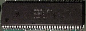
The YM2610 is a sound synthesis chip made by Yamaha, | The YM2610 is a sound synthesis and playback chip made by Yamaha, found in all versions of the NeoGeo hardware. | ||
It was later merged with | It was later merged with other chips in {{Chipname|NEO-YSA}} and {{Chipname|NEO-YSA2}}, which are used on some versions of the NeoGeo CD, the [[CDZ]], the {{PCB|MV1C}} and on [[ROM-Only boards]]. | ||
The chip | The YM2610 requires a {{Chipname|YM3016}} external DAC (Digital to Analog Converter) chip for the [[FM]] and [[ADPCM]] sounds. The only direct analog output is for the [[SSG]] mono sounds. Both analog signals are then mixed together before amplification. | ||
The original YM2610 chip gets quite warm during normal operation. | |||
=Parts= | |||
Sound comes from 3 different generators, each having their own channels: | |||
* | * [[SSG]] (Software Sound Generator): 3 channels | ||
* | * [[FM]] (Frequency Modulation): 4 channels | ||
* | * [[ADPCM]] (Sample playback): 7 channels | ||
Providing 14 channels in total. | |||
= | =Programming= | ||
See [[Z80/YM2610 interface]] and [[YM2610 registers]]. | |||
=Pinout= | |||
[[File:Ym2610_pinout.png|right|640px]] | |||
* {{Sig|SDD|SDD*}}: {{Chipname|Z80}} data bus | |||
* {{Sig|RAD|RAD*}}: ADPCM-A multiplexed address/data | |||
* {{Sig|RMPX|RMPX}}: ADPCM-A address/data select | |||
* {{Sig|ROE|ROE}}: APDCM-A data output enable | |||
* {{Sig|RA|RA*}}: ADPCM-A address | |||
* {{Sig|ANA|ANA}}: SSG analog output | |||
* {{Sig|SH1|SH1}}: {{Chipname|YM3016}} latch 1 | |||
* {{Sig|SH2|SH2}}: YM3016 latch 2 | |||
* {{Sig|OP0|OP0}}: YM3016 serial data | |||
* {{Sig|PA|PA*}}: ADPCM-B address | |||
* {{Sig|POE|POE}}: ADPCM-B data output enable | |||
* {{Sig|PMPX|PMPX}}: ADPCM-B address/data select | |||
* {{Sig|PAD|PAD*}}: ADPCM-B multiplexed address/data | |||
* {{Sig|IRQ|IRQ}}: Interrupt request output | |||
* {{Sig|CS|CS}}: Chip select | |||
* {{Sig|WR|WR}}: Write | |||
* {{Sig|RD|RD}}: Read | |||
* {{Sig|SDA|A*}}: Z80 address bus | |||
* {{Sig|PHI M|PHI M}}: [[Clock]] input | |||
* {{Sig|PHI S|PHI S}}: YM3016 clock output | |||
<br clear="right"/> | |||
== | =Multiplexed ADPCM bus= | ||
Access to the [[V ROM]]s are made via partly multiplexed buses. See [[YM2610 bus timing]] for more details about the access sequences. | |||
The | The {{Sig|SDRMPX|SDRMPX}} and {{Sig|SDPMPX|SDPMPX}} signals are used to control latches or the {{Chipname|PCM}} chip in [[cartridges]] to demultiplex address and data. When {{Sig|SDROE|SDROE}} or {{Sig|SDPOE|SDPOE}} goes low, SDRAD* and SDPAD* are tristated so that the V ROMs can output data. | ||
* SDRA* for ADPCM-A | |||
=== | {|class="wikitable" | ||
!rowspan="2"|SDRMPX edge | |||
!colspan="8"|SDRAD* | |||
!colspan="6"|SDRA* | |||
|- | |||
!0 | |||
!1 | |||
!2 | |||
!3 | |||
!4 | |||
!5 | |||
!6 | |||
!7 | |||
!8 | |||
!9 | |||
!20 | |||
!21 | |||
!22 | |||
!23 | |||
|- | |||
|Low to high | |||
|0 | |||
|1 | |||
|2 | |||
|3 | |||
|4 | |||
|5 | |||
|6 | |||
|7 | |||
|8 | |||
|9 | |||
|? | |||
|? | |||
|? | |||
|? | |||
|- | |||
|High to low | |||
|10 | |||
|11 | |||
|12 | |||
|13 | |||
|14 | |||
|15 | |||
|16 | |||
|17 | |||
|18 | |||
|19 | |||
|20 | |||
|21 | |||
|22 | |||
|23 | |||
|} | |||
* SDPA* for ADPCM-B | |||
=== | {|class="wikitable" | ||
!rowspan="2"|SDPMPX edge | |||
!colspan="8"|SDPAD* | |||
!colspan="6"|SDPA* | |||
|- | |||
!0 | |||
!1 | |||
!2 | |||
!3 | |||
!4 | |||
!5 | |||
!6 | |||
!7 | |||
!8 | |||
!9 | |||
!10 | |||
!11 | |||
|- | |||
|Low to high | |||
|0 | |||
|1 | |||
|2 | |||
|3 | |||
|4 | |||
|5 | |||
|6 | |||
|7 | |||
|8 | |||
|9 | |||
|10 | |||
|11 | |||
|- | |||
|High to low | |||
|12 | |||
|13 | |||
|14 | |||
|15 | |||
|16 | |||
|17 | |||
|18 | |||
|19 | |||
|20 | |||
|21 | |||
|22 | |||
|23 | |||
|} | |||
24 address bits allow for 16MiB max V ROMs (without bankswitching). | |||
=Trivia= | |||
* A lot of games have several recordings of the same instrument playing different notes, rather than having only one sample and change the ADPCM-B playback frequency to vary its pitch. (Trumpet in [[Viewpoint]], electric guitar in [[Super Sidekicks]]). Why ? | |||
* Nazca's [[sound driver]]s are able to use the SSG channels for music playback. (Maybe all can ?) | |||
= | =Datasheet= | ||
Japanese datasheet: [[http://www.ajworld.net/neogeodev/ym2610am_en.html ajworld.net]] | |||
Incomplete/translated datasheet: [[http://furrtek.free.fr/noclass/neogeo/YM2610.pdf YM2610.pdf]] | Incomplete/translated datasheet: [[http://furrtek.free.fr/noclass/neogeo/YM2610.pdf YM2610.pdf]] | ||
Latest revision as of 18:19, 26 July 2017

| |
| Package | SDIP64 |
| Manufacturer | |
| First use | 1990 ? |
| Used on | All systems |
The YM2610 is a sound synthesis and playback chip made by Yamaha, found in all versions of the NeoGeo hardware. It was later merged with other chips in NEO-YSA and NEO-YSA2, which are used on some versions of the NeoGeo CD, the CDZ, the MV1C and on ROM-Only boards.
The YM2610 requires a YM3016 external DAC (Digital to Analog Converter) chip for the FM and ADPCM sounds. The only direct analog output is for the SSG mono sounds. Both analog signals are then mixed together before amplification.
The original YM2610 chip gets quite warm during normal operation.
Parts
Sound comes from 3 different generators, each having their own channels:
- SSG (Software Sound Generator): 3 channels
- FM (Frequency Modulation): 4 channels
- ADPCM (Sample playback): 7 channels
Providing 14 channels in total.
Programming
See Z80/YM2610 interface and YM2610 registers.
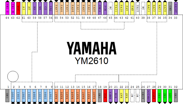
Pinout

- SDD: Z80 data bus
- RAD: ADPCM-A multiplexed address/data
- RMPX: ADPCM-A address/data select
- ROE: APDCM-A data output enable
- RA: ADPCM-A address
- ANA: SSG analog output
- SH1: YM3016 latch 1
- SH2: YM3016 latch 2
- OP0: YM3016 serial data
- PA: ADPCM-B address
- POE: ADPCM-B data output enable
- PMPX: ADPCM-B address/data select
- PAD: ADPCM-B multiplexed address/data
- IRQ: Interrupt request output
- CS: Chip select
- WR: Write
- RD: Read
- SDA: Z80 address bus
- PHI M: Clock input
- PHI S: YM3016 clock output
Multiplexed ADPCM bus
Access to the V ROMs are made via partly multiplexed buses. See YM2610 bus timing for more details about the access sequences.
The SDRMPX and SDPMPX signals are used to control latches or the PCM chip in cartridges to demultiplex address and data. When SDROE or SDPOE goes low, SDRAD* and SDPAD* are tristated so that the V ROMs can output data.
- SDRA* for ADPCM-A
| SDRMPX edge | SDRAD* | SDRA* | ||||||||||||
|---|---|---|---|---|---|---|---|---|---|---|---|---|---|---|
| 0 | 1 | 2 | 3 | 4 | 5 | 6 | 7 | 8 | 9 | 20 | 21 | 22 | 23 | |
| Low to high | 0 | 1 | 2 | 3 | 4 | 5 | 6 | 7 | 8 | 9 | ? | ? | ? | ? |
| High to low | 10 | 11 | 12 | 13 | 14 | 15 | 16 | 17 | 18 | 19 | 20 | 21 | 22 | 23 |
- SDPA* for ADPCM-B
| SDPMPX edge | SDPAD* | SDPA* | ||||||||||||
|---|---|---|---|---|---|---|---|---|---|---|---|---|---|---|
| 0 | 1 | 2 | 3 | 4 | 5 | 6 | 7 | 8 | 9 | 10 | 11 | |||
| Low to high | 0 | 1 | 2 | 3 | 4 | 5 | 6 | 7 | 8 | 9 | 10 | 11 | ||
| High to low | 12 | 13 | 14 | 15 | 16 | 17 | 18 | 19 | 20 | 21 | 22 | 23 | ||
24 address bits allow for 16MiB max V ROMs (without bankswitching).
Trivia
- A lot of games have several recordings of the same instrument playing different notes, rather than having only one sample and change the ADPCM-B playback frequency to vary its pitch. (Trumpet in Viewpoint, electric guitar in Super Sidekicks). Why ?
- Nazca's sound drivers are able to use the SSG channels for music playback. (Maybe all can ?)
Datasheet
Japanese datasheet: [ajworld.net]
Incomplete/translated datasheet: [YM2610.pdf]