NEO-253: Difference between revisions
Jump to navigation
Jump to search
mNo edit summary |
(Finished MV4F pinouts) |
||
| (3 intermediate revisions by the same user not shown) | |||
| Line 1: | Line 1: | ||
{{ChipInfo | |||
|picture=Neo-253.jpg | |||
|pkg=QFP64R | |||
|manu=fujitsu | |||
|date=1992 ? | |||
|gates= | |||
|used_on={{PCB|SLOT4F}} | |||
}} | |||
Quintuple 74HC253 4-to-1 multiplexers with common select lines, making | Quintuple 74HC253 4-to-1 multiplexers with common select lines, making ten 4-to-1 switches in one chip. Used to switch read-only buses. The inputs are named according to the related slot: A is slot #1, B is slot #2... | ||
Only (?) used on second revision 4-slot MVS systems. Not to be confused with the more common {{Chipname|NEO-273}}. | |||
=Pinout= | |||
[[File:Neo-253_pinout.png|512px]] | [[File:Neo-253_pinout.png|512px]] | ||
| Line 14: | Line 18: | ||
OpenOffice Draw file: [[File:neo-253.odg]] | OpenOffice Draw file: [[File:neo-253.odg]] | ||
Select signals come from {{Chipname|NEO-F0}} SLOTA and SLOTB. | |||
==SLOT4F @ 5E== | |||
Cartridge [[wait cycle]] configuration and [[Z80]] bus. | |||
*Mux 1: PWAIT0 | |||
*Mux 2: PWAIT1 | |||
*Mux 10~3: SDD7~SDD0 | |||
Outputs go to CN9. | |||
==SLOT4F @ 5D== | |||
[[Sprites]] and [[fix layer]] graphics. | |||
*Mux 1: CR30 | |||
*Mux 2: CR31 | |||
*Mux 10~3: FIXD7~FIXD0 | |||
==SLOT4F @ 5C== | |||
Sprite graphics. | |||
*Mux 10~1: CR29~CR20 | |||
==SLOT4F @ 5B== | |||
Sprite graphics. | |||
*Mux 10~1: CR19~CR10 | |||
==SLOT4F @ 5A== | |||
Sprite graphics. | |||
*Mux 10~1: CR9~CR0 | |||
[[Category:Chips]] | [[Category:Chips]] | ||
Latest revision as of 17:07, 18 September 2017

| |
| Package | QFP64R |
| Manufacturer | |
| First use | 1992 ? |
| Used on | SLOT4F |
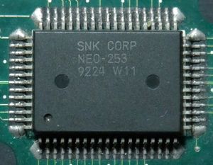
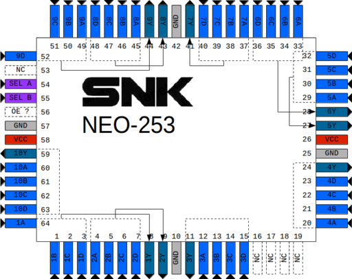
Quintuple 74HC253 4-to-1 multiplexers with common select lines, making ten 4-to-1 switches in one chip. Used to switch read-only buses. The inputs are named according to the related slot: A is slot #1, B is slot #2...
Only (?) used on second revision 4-slot MVS systems. Not to be confused with the more common NEO-273.
Pinout
OpenOffice Draw file: File:Neo-253.odg
Select signals come from NEO-F0 SLOTA and SLOTB.
SLOT4F @ 5E
Cartridge wait cycle configuration and Z80 bus.
- Mux 1: PWAIT0
- Mux 2: PWAIT1
- Mux 10~3: SDD7~SDD0
Outputs go to CN9.
SLOT4F @ 5D
Sprites and fix layer graphics.
- Mux 1: CR30
- Mux 2: CR31
- Mux 10~3: FIXD7~FIXD0
SLOT4F @ 5C
Sprite graphics.
- Mux 10~1: CR29~CR20
SLOT4F @ 5B
Sprite graphics.
- Mux 10~1: CR19~CR10
SLOT4F @ 5A
Sprite graphics.
- Mux 10~1: CR9~CR0
