Pinouts: Difference between revisions
Jump to navigation
Jump to search
mNo edit summary |
m (→MVS boards) |
||
| (22 intermediate revisions by 3 users not shown) | |||
| Line 1: | Line 1: | ||
= | =A/V connector= | ||
[[File:Av_pinout.png]] | |||
Note: Some home consoles revisions appear to only provide composite video, no separate sync signal. | |||
= | =Cartridges= | ||
* [[AES cartridge pinout]] | |||
* [[MVS cartridge pinout]] | |||
=Joypad ports= | =[[Joypad]] ports= | ||
Inputs are pulled high to +5V. | Special, deep DA-15 connectors with a plastic shield. 10 direct inputs, 3 outputs, 2 power lines. | ||
Inputs are pulled high to +5V by [[CRE401]] R-C arrays. | |||
Outputs are open collector through 22 ohms resistors (not pulled high). | |||
<center>[[File:Joypad_pinout.png]]</center> | <center>[[File:Joypad_pinout.png]]</center> | ||
=JAMMA connector= | =JAMMA= | ||
See [[JAMMA connector pinout]]. | |||
=Memory card= | |||
See [[Memory card pinout]]. | |||
=MVS boards= | |||
[[MV4]] | |||
* [[MVS board connectors pinouts|MVS MV-4 board connectors pinouts]]. | |||
[[MV6]] | |||
* [[MVS MV-6 daughter board connectors pinouts]]. | |||
=[[Multiplayer]] jack= | |||
RS-485 pair + ground. Use a stereo cable only ! | |||
* Sleeve: Ground | |||
* Ring: D- | |||
* Tip: D+ | |||
=CD/CDZ= | =CD/CDZ= | ||
==Power supply connector== | |||
[[File:Cdpow_pinout.png]] | |||
See [[power supply]]. | |||
==YM2610 digital audio== | ==YM2610 digital audio== | ||
[[File: | [[File:Cd2_cn6.jpg|Cd2_cn6.jpg]] | ||
# OP0 | |||
# PHI | |||
# SH2 | |||
# SH1 | |||
# Analog | |||
==Video and CDDA== | ==Video and CDDA== | ||
[[File:Cd2_cn1cn3.jpg|400px]] | [[File:Cd2_cn1cn3.jpg|400px]] | ||
==CD | Video: | ||
# Red | |||
# Green | |||
# Blue | |||
# Sync | |||
# Burst | |||
# GND | |||
CDDA: | |||
# LRCK | |||
# DATA | |||
# BCLK | |||
==CD drive== | |||
[[File:Cd2_cn4.jpg|400px]] | [[File:Cd2_cn4.jpg|400px]] | ||
See [[CD drive]]. | |||
== | ==PCB power== | ||
[[File:Cd2_cn5.jpg]] | [[File:Cd2_cn5.jpg]] | ||
= | # <span style="color:#7F007F;">Purple: 5V CD</span> | ||
# <span style="color:#BF7F00;">Yellow: 10V CD</span> | |||
# <span style="color:#FF0000;">Red: 5V logic</span> | |||
# Black: Ground | |||
[[Category:Chips]] | [[Category:Chips]] | ||
[[Category:Base system]] | [[Category:Base system]] | ||
Latest revision as of 15:30, 3 May 2021
A/V connector
Note: Some home consoles revisions appear to only provide composite video, no separate sync signal.
Cartridges
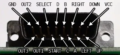
Joypad ports
Special, deep DA-15 connectors with a plastic shield. 10 direct inputs, 3 outputs, 2 power lines.
Inputs are pulled high to +5V by CRE401 R-C arrays.
Outputs are open collector through 22 ohms resistors (not pulled high).

JAMMA
Memory card
See Memory card pinout.
MVS boards
Multiplayer jack
RS-485 pair + ground. Use a stereo cable only !
- Sleeve: Ground
- Ring: D-
- Tip: D+
CD/CDZ
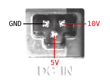
Power supply connector
See power supply.
YM2610 digital audio
- OP0
- PHI
- SH2
- SH1
- Analog
Video and CDDA
Video:
- Red
- Green
- Blue
- Sync
- Burst
- GND
CDDA:
- LRCK
- DATA
- BCLK
CD drive
File:Cd2 cn4.jpg See CD drive.
PCB power
- Purple: 5V CD
- Yellow: 10V CD
- Red: 5V logic
- Black: Ground

