|
|
| (17 intermediate revisions by 2 users not shown) |
| Line 1: |
Line 1: |
| | =A/V connector= |
| | |
| | [[File:Av_pinout.png]] |
| | |
| | Note: Some home consoles revisions appear to only provide composite video, no separate sync signal. |
| | |
| =Cartridges= | | =Cartridges= |
| ==Signal names==
| |
|
| |
|
| *6M, 12M, 24M: 6MHz, 12MHz, and 24MHz clock signals | | * [[AES cartridge pinout]] |
| *4MB: 4MHz inverted signal
| | * [[MVS cartridge pinout]] |
| *A1~A19: [[68k]] address bus
| | |
| *D0~D15: 68k data bus
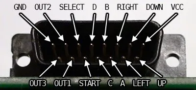
| | =[[Joypad]] ports= |
| *R/W: 68k R/W
| | |
| *AS: 68k /AS
| | Special, deep DA-15 connectors with a plastic shield. 10 direct inputs, 3 outputs, 2 power lines. |
| */ROMOEL: $000000-$0FFFFF odd byte read
| | |
| */ROMOEU: $000000-$0FFFFF even byte read
| | Inputs are pulled high to +5V by [[CRE401]] R-C arrays in the systems. |
| */ROMOE: $000000-$0FFFFF read
| |
| */PORTOEL: $200000-$2FFFFF odd byte read
| |
| */PORTOEU: $200000-$2FFFFF even byte read
| |
| */PORTWEL: $200000-$2FFFFF odd byte write
| |
| */PORTWEU: $200000-$2FFFFF even byte write
| |
| */PORTADRS: $200000-$2FFFFF any access
| |
| *CR0~CR31: [[C ROM]]s data bus (2*16bits) | |
| *SDRAD0~SDRAD7: ADPCM-A ROM [[YM2610#Multiplexed bus|multiplexed bus]] (data/address)
| |
| *SDRA8,SDRA9,SDRA20~SDRA23: ADPCM-A ROM address bus
| |
| *SDPAD0~SDPAD7: ADPCM-B ROM multiplexed bus (data/address)
| |
| *SDPA8,SDPA9,SDPA10,SDPA11: ADPCM-B ROM address bus
| |
| *P0~P23: C ROM and [[S ROM]] address bus (multiplexed)
| |
| *PCK1B: Clock to latch C ROM address from P0~P23 ([[NEO-273|mapping]]) on rising edge
| |
| *PCK2B: Clock to latch S ROM address from P0~P15 ([[NEO-273|mapping]]) on rising edge
| |
| *CA4: C ROM A4
| |
| *2H1: S ROM A3
| |
| *FIXD0~FIXD7: S ROM data bus
| |
|
| |
|
| ==AES Cartridge==
| | Outputs are open collector through 22 ohms resistors (not pulled high). |
|
| |
|
| {| class="regdef" align="center" style="text-align:center;align:right;"
| | <center>[[File:Joypad_pinout.png]]</center> |
| |PROG
| |
| |CHA
| |
| |-
| |
| |[[File:aesprogpinout.png]]
| |
| |[[File:aeschapinout.png]]
| |
| |}
| |
|
| |
|
| *: Audio loops only used on NEO-AES systems (info from [[User:Kyuusaku]])
| | =JAMMA= |
|
| |
|
| ==MVS Cartridge==
| | See [[JAMMA connector pinout]]. |
|
| |
|
| {| class="regdef" align="center" style="text-align:center;align:right;"
| | =Memory card= |
| |CHA bottom
| |
| |CHA top
| |
| |PROG bottom
| |
| |PROG top
| |
| |-
| |
| |[[File:mvscartchabot.png|200px]]
| |
| |[[File:mvscartchatop.png|200px]]
| |
| |[[File:mvscartprgbot.png|200px]]
| |
| |[[File:mvscartprgtop.png|200px]]
| |
| |}
| |
|
| |
|
| | See [[Memory card pinout]]. |
|
| |
|
| <span style="color:#FF0000"><B>Beware !</B> Pinouts found elsewhere have ROMOE/4MB swapped, it's an error on the original schematics. ROMOE is on pin 33 bottom, 4MB is on pin 34 bottom.</span>
| | =MVS boards= |
|
| |
|
| possible correction (delete this text whenever): "SYSTEMB" appears to actually be a slot selection pin.
| | [[MV4]] |
| *On MV-2F, slot 1 A42 is connected to NEO-F0 SLOT0
| |
| *slot 2 A42 is connected to NEO-F0 SLOT1
| |
| Makes sense for 1F schematics to connect it straight to SYSTEMB since there are no other possible slots. On multislot, it comes from NEO-F0 (or equivalent) SLOT* outputs. NEO-F0 has SYSTEMB as an input so it probably only has SLOT* pins active when the cart ROMs are selected.
| |
|
| |
|
| =Joypad ports=
| | * [[MVS board connectors pinouts|MVS MV-4 board connectors pinouts]]. |
|
| |
|
| Inputs are pulled high to +5V.
| | [[MV6]] |
|
| |
|
| <center>[[File:Joypad_pinout.png]]</center>
| | * [[MVS MV-6 daughter board connectors pinouts]]. |
|
| |
|
| =JAMMA connector= | | =[[Multiplayer]] jack= |
| Infos from [[http://www.hardmvs.com HardMVS.com]]
| |
|
| |
|
| {| class="regdef"
| | RS-485 pair + ground. Use a stereo cable only ! |
| |bgcolor="#DDDDDD"|GND
| |
| |'''A'''
| |
| |'''1'''
| |
| |bgcolor="#DDDDDD"|GND
| |
| |-
| |
| |bgcolor="#DDDDDD"|GND
| |
| |'''B'''
| |
| |'''2'''
| |
| |bgcolor="#DDDDDD"|GND
| |
| |-
| |
| |bgcolor="#DD8888"| +5V
| |
| |'''C'''
| |
| |'''3'''
| |
| |bgcolor="#DD8888"| +5V
| |
| |-
| |
| |bgcolor="#DD8888"| +5V
| |
| |'''D'''
| |
| |'''4'''
| |
| |bgcolor="#DD8888"| +5V
| |
| |-
| |
| |
| |
| |'''E'''
| |
| |'''5'''
| |
| |
| |
| |-
| |
| |bgcolor="#DDDD88"| +12V
| |
| |'''F'''
| |
| |'''6'''
| |
| |bgcolor="#DDDD88"| +12V
| |
| |-
| |
| |Key
| |
| |'''H'''
| |
| |'''7'''
| |
| |Key
| |
| |-
| |
| |Coin counter #2
| |
| |'''J'''
| |
| |'''8'''
| |
| |Coin counter #1
| |
| |-
| |
| |Lockout coil #2
| |
| |'''K'''
| |
| |'''9'''
| |
| |Lockout coil #1
| |
| |-
| |
| |bgcolor="#DD8844"|Left speaker +
| |
| |'''L'''
| |
| |'''10'''
| |
| |bgcolor="#DD8844"|Right speaker +
| |
| |-
| |
| |Test switch
| |
| |'''M'''
| |
| |'''11'''
| |
| |bgcolor="#DD8844"|Mono audio +
| |
| |-
| |
| |bgcolor="#44FF44"|Video green
| |
| |'''N'''
| |
| |'''12'''
| |
| |bgcolor="#FF4444"|Video red
| |
| |-
| |
| |bgcolor="#FFFF44"|Video sync
| |
| |'''P'''
| |
| |'''13'''
| |
| |bgcolor="#4444FF"|Video blue
| |
| |-
| |
| |Service switch
| |
| |'''R'''
| |
| |'''14'''
| |
| |bgcolor="#DDDDDD"|Video GND
| |
| |-
| |
| |Coin switch #4 P2
| |
| |'''S'''
| |
| |'''15'''
| |
| |Coin switch #3 P1
| |
| |-
| |
| |Coin switch #2 P2
| |
| |'''T'''
| |
| |'''16'''
| |
| |Coin switch #1 P1
| |
| |-
| |
| |P2 Start
| |
| |'''U'''
| |
| |'''17'''
| |
| |P1 Start
| |
| |-
| |
| |P2 Up
| |
| |'''V'''
| |
| |'''18'''
| |
| |P1 Up
| |
| |-
| |
| |P2 Down
| |
| |'''W'''
| |
| |'''19'''
| |
| |P1 Down
| |
| |-
| |
| |P2 Left
| |
| |'''X'''
| |
| |'''20'''
| |
| |P1 Left
| |
| |-
| |
| |P2 Right
| |
| |'''Y'''
| |
| |'''21'''
| |
| |P1 Right
| |
| |-
| |
| |P2 A
| |
| |'''Z'''
| |
| |'''22'''
| |
| |P1 A
| |
| |-
| |
| |P2 B
| |
| |'''a'''
| |
| |'''23'''
| |
| |P1 B
| |
| |-
| |
| |P2 C
| |
| |'''b'''
| |
| |'''24'''
| |
| |P1 C
| |
| |-
| |
| |P2 D
| |
| |'''c'''
| |
| |'''25'''
| |
| |P1 D
| |
| |-
| |
| |Select down
| |
| |'''d'''
| |
| |'''26'''
| |
| |Select up
| |
| |-
| |
| |bgcolor="#DDDDDD"|GND
| |
| |'''e'''
| |
| |'''27'''
| |
| |bgcolor="#DDDDDD"|GND
| |
| |-
| |
| |bgcolor="#DDDDDD"|GND
| |
| |'''f'''
| |
| |'''28'''
| |
| |bgcolor="#DDDDDD"|GND
| |
| |}
| |
|
| |
|
| | * Sleeve: Ground |
| | * Ring: D- |
| | * Tip: D+ |
|
| |
|
| =CD/CDZ= | | =CD/CDZ= |
| | |
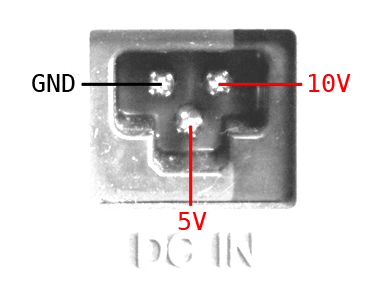
| | ==Power supply connector== |
| | |
| | [[File:Cdpow_pinout.png]] |
| | |
| | See [[power supply]]. |
|
| |
|
| ==YM2610 digital audio== | | ==YM2610 digital audio== |
| [[File:Cd2_cn7.jpg|Cd2_cn7.jpg]] | | [[File:Cd2_cn6.jpg|Cd2_cn6.jpg]] |
| Clock, L, R ?
| | |
| | # OP0 |
| | # PHI |
| | # SH2 |
| | # SH1 |
| | # Analog |
|
| |
|
| ==Video and CDDA== | | ==Video and CDDA== |
| [[File:Cd2_cn1cn3.jpg|400px]] | | [[File:Cd2_cn1cn3.jpg|400px]] |
| R, V, B, S, Burst, GND ?
| |
| Clock, L, R ?
| |
|
| |
|
| ==CD reader== | | Video: |
| | # Red |
| | # Green |
| | # Blue |
| | # Sync |
| | # Burst |
| | # GND |
| | |
| | CDDA: |
| | # LRCK |
| | # DATA |
| | # BCLK |
| | |
| | ==CD drive== |
| [[File:Cd2_cn4.jpg|400px]] | | [[File:Cd2_cn4.jpg|400px]] |
| | See [[CD drive]]. |
|
| |
|
| ==Power== | | ==PCB power== |
| [[File:Cd2_cn5.jpg]] | | [[File:Cd2_cn5.jpg]] |
|
| |
|
| =Multiplayer jack= | | # <span style="color:#7F007F;">Purple: 5V CD</span> |
| To do.
| | # <span style="color:#BF7F00;">Yellow: 10V CD</span> |
| | | # <span style="color:#FF0000;">Red: 5V logic</span> |
| | # Black: Ground |
|
| |
|
| [[Category:Chips]] | | [[Category:Chips]] |
| [[Category:Base system]] | | [[Category:Base system]] |


