Memory card: Difference between revisions
m (→Header) |
|||
| (8 intermediate revisions by 2 users not shown) | |||
| Line 1: | Line 1: | ||
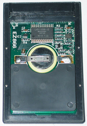
[[File:snkmemcard.jpg|thumb|SRAM memory card, showing the SRAM chip and voltage detection circuit. Picture by [[User:HPMAN|HPMAN]]]] | [[File:snkmemcard.jpg|thumb|SRAM memory card, showing the SRAM chip and voltage detection circuit. Picture by [[User:HPMAN|HPMAN]]]] | ||
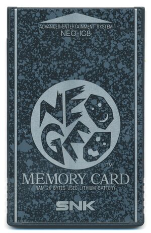
[[File:NEO-IC8_front.jpg|thumb|NEO-IC8, original SNK card. Picture by [[User:ArcadeTV|ArcadeTV]]]] | |||
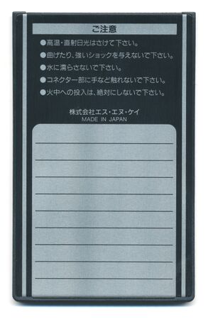
[[File:NEO-IC8_back.jpg|thumb|NEO-IC8, back of original SNK card. Picture by [[User:ArcadeTV|ArcadeTV]]]] | |||
The | The NeoGeo home console and some [[MVS hardware|MVS]] cabs can use [[JEIDA V3]] memory cards to store game saves and/or high scores, allowing players to save their progress and continue on any system running the same game. | ||
Even if the memory card [[68k memory map|address space]] can be freely used, games should only perform memory card operations through the [[CARD]] system ROM call to avoid data corruption. | |||
=Supported card types= | |||
The SP-S2 [[system ROM]] (and probably all the others) can handle 8 memory card sizes from 2KiB up to 16KiB, in 2KiB steps: | |||
*2KiB | |||
*4KiB | |||
*6KiB | |||
*8KiB | |||
*10KiB | |||
*14KiB | |||
*16KiB | |||
And 4 different card types: | |||
*8 bits wide | |||
*16 bits wide | |||
*16 bits wide "doubled" | |||
*"SNK ROM" cards | |||
For 8-bit cards (all official SNK cards ?) only the lower byte is used, but accesses must '''always''' be done in words. This is because memory card accesses are only enabled for word or upper byte operations (/UDS 68k signal). | |||
=Original SNK card= | |||
The original SNK-branded memory card was a [[:File:CR2016_battery.jpg|battery-backed]] 8-bit wide 2KiB card using a [[LH5116|LH5116 SRAM chip]] and voltage switching circuitry. | |||
Since it uses a battery, it may be prone to data loss if the voltage drops below 2V. Unlike the MVS [[backup RAM]] battery, the memory card one isn't rechargeable. | |||
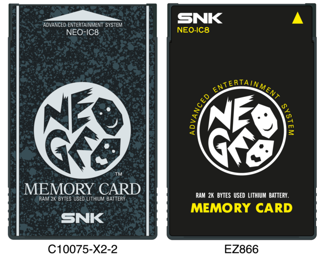
There are at least 2 known versions of the original SNK Memory Card, each with its individual design and circuit-board:<br> | |||
[[Image:NEO-IC8_versions.png|640px]] | |||
The first version has the [[C10075-X2-2]] while the later one hase the [[EZ866]] board. | |||
=CD systems= | |||
A "virtual" memory card is embedded in [[CD systems]] as a 8KiB battery-backed SRAM chip. | |||
=Data format= | =Data format= | ||
All cards use the same format regardless of capacity, only regions sizes differ. Since the JEIDA data bus is 16-bits wide, make sure to double the address for 8-bit cards if you choose to access their memory directly. | |||
The data is referred to as "blocks", one block being 64 bytes. The header always occupies the first block. Eg. A 2KiB card can hold (2048/64)-1 = 31 blocks. | |||
The data is split into 5 regions: | The data is split into 5 regions: | ||
| Line 17: | Line 52: | ||
==Header== | ==Header== | ||
Always | Always 64 bytes. | ||
{| class=" | {|class="wikitable" | ||
| '''Address''' | | '''Address''' | ||
| '''Name''' | | '''Name''' | ||
| Line 35: | Line 70: | ||
|CARD_SIZE | |CARD_SIZE | ||
|word | |word | ||
| | |Address space used by the memory card. Eg. A 2KiB 8-bit card is $1000. | ||
|- | |- | ||
|$C | |$C | ||
| Line 75: | Line 110: | ||
==Directory== | ==Directory== | ||
List of saves of 32, 64, 96, 128, 160, 192, 224 or 256 entries. The size depends on the card's capacity. | List of saves of 32, 64, 96, 128, 160, 192, 224 or 256 entries. The size depends on the card's capacity. | ||
Each entry | Note that since the header occupies the first block, there will always be at least one unused directory entry. | ||
Each entry is 4 bytes, with the following format: | |||
{| class="regdef" | {| class="regdef" | ||
| Line 86: | Line 123: | ||
|$0 | |$0 | ||
|byte | |byte | ||
|Save sub number (CARD_SUB), 0 to 15. $FF if entry is free. | |Save sub-number (CARD_SUB), 0 to 15. $FF if entry is free. | ||
|- | |- | ||
|$1 | |$1 | ||
| Line 94: | Line 131: | ||
|$3 | |$3 | ||
|byte | |byte | ||
|FAT entry | |FAT entry index (see below) | ||
|} | |} | ||
==FAT 1== | ==FAT 1== | ||
List of used blocks | List of used blocks of 64, 128, 192, or 256 entries. The size depends on the card's capacity. | ||
* $02 is a block | * $02 is a block reserved by the system ROM | ||
* $01 is a block used by a game | * $01 is a block used by a game | ||
* $00 is a free block | * $00 is a free block | ||
| Line 107: | Line 144: | ||
FAT 2 is simply a mirror of FAT 1. | FAT 2 is simply a mirror of FAT 1. | ||
If any of the FAT tables checksum is bad, the correct table is written over the other one. If both checksums are bad, the system ROM displays an error. | |||
==Game Data== | ==Game Data== | ||
Many games use | Many games use only one block, but some may use more. | ||
The first 20 bytes | The first 20 bytes contain the data title (usually the game and stage name). | ||
=Registers= | =Registers= | ||
* Write is enabled if {{Reg|REG_CRDUNLOCK1}} | * Write is enabled if {{Reg|REG_CRDUNLOCK1}} and {{Reg|REG_CRDUNLOCK2}} are written to | ||
* The WP (Write Protect) pin is read through bit 6 of {{Reg|REG_STATUS_B}} | * The WP (Write Protect) pin is read through bit 6 of {{Reg|REG_STATUS_B}} | ||
* CD1 (Card Detect 1) is read through bit 4 of {{Reg|REG_STATUS_B}} | * CD1 (Card Detect 1) is read through bit 4 of {{Reg|REG_STATUS_B}} | ||
* CD2 (Card Detect 2) is read through bit 5 of {{Reg|REG_STATUS_B}} | * CD2 (Card Detect 2) is read through bit 5 of {{Reg|REG_STATUS_B}} | ||
* Attribute memory is selected if {{Reg|REG_CRDREGSEL}} is | ** Both must be 0 if the card is inserted correctly | ||
* Attribute memory is selected if {{Reg|REG_CRDREGSEL}} is written to, never used ? | |||
= | =Pinout= | ||
See [[Memory card pinout]]. | |||
[[Category:Cartridge systems]] | [[Category:Cartridge systems]] | ||
Latest revision as of 01:25, 17 January 2023


The NeoGeo home console and some MVS cabs can use JEIDA V3 memory cards to store game saves and/or high scores, allowing players to save their progress and continue on any system running the same game.
Even if the memory card address space can be freely used, games should only perform memory card operations through the CARD system ROM call to avoid data corruption.
Supported card types
The SP-S2 system ROM (and probably all the others) can handle 8 memory card sizes from 2KiB up to 16KiB, in 2KiB steps:
- 2KiB
- 4KiB
- 6KiB
- 8KiB
- 10KiB
- 14KiB
- 16KiB
And 4 different card types:
- 8 bits wide
- 16 bits wide
- 16 bits wide "doubled"
- "SNK ROM" cards
For 8-bit cards (all official SNK cards ?) only the lower byte is used, but accesses must always be done in words. This is because memory card accesses are only enabled for word or upper byte operations (/UDS 68k signal).
Original SNK card
The original SNK-branded memory card was a battery-backed 8-bit wide 2KiB card using a LH5116 SRAM chip and voltage switching circuitry.
Since it uses a battery, it may be prone to data loss if the voltage drops below 2V. Unlike the MVS backup RAM battery, the memory card one isn't rechargeable.
There are at least 2 known versions of the original SNK Memory Card, each with its individual design and circuit-board:

The first version has the C10075-X2-2 while the later one hase the EZ866 board.
CD systems
A "virtual" memory card is embedded in CD systems as a 8KiB battery-backed SRAM chip.
Data format
All cards use the same format regardless of capacity, only regions sizes differ. Since the JEIDA data bus is 16-bits wide, make sure to double the address for 8-bit cards if you choose to access their memory directly.
The data is referred to as "blocks", one block being 64 bytes. The header always occupies the first block. Eg. A 2KiB card can hold (2048/64)-1 = 31 blocks.
The data is split into 5 regions:
Header
Always 64 bytes.
| Address | Name | Size | Description |
| $0~$9 | 10 bytes | Zeros or "SNK ROM " (development unit ?)
For 16 bits "doubled" cards, $6 is set to $0001 | |
| $A | CARD_SIZE | word | Address space used by the memory card. Eg. A 2KiB 8-bit card is $1000. |
| $C | byte | 0 | |
| $D | CARD_FAT_1_CHKSUM | byte | Checksum of FAT 1 |
| $E | CARD_FAT_2_CHKSUM | byte | Checksum of FAT 2 |
| $F | CARD_USERNAME_AVAILABLE | byte | 0 : Username unavailable, !0 : Username available |
| $10 | CARD_USERNAME | 16 bytes | Card holder's username |
| $20 | CARD_MAGIC | 16 bytes | $4E $XX $45 $XX $4F $XX $2D $XX $47 $XX $45 $XX $4F $XX $80 $XX ("NEO-GEO", $80) |
| $30 | CARD_REGION | byte | Region of the system that formated the card, 0 = Japan, 1 = USA, 2 = Europe |
Directory
List of saves of 32, 64, 96, 128, 160, 192, 224 or 256 entries. The size depends on the card's capacity.
Note that since the header occupies the first block, there will always be at least one unused directory entry.
Each entry is 4 bytes, with the following format:
| Address | Size | Description |
| $0 | byte | Save sub-number (CARD_SUB), 0 to 15. $FF if entry is free. |
| $1 | word | Game's NGH number |
| $3 | byte | FAT entry index (see below) |
FAT 1
List of used blocks of 64, 128, 192, or 256 entries. The size depends on the card's capacity.
- $02 is a block reserved by the system ROM
- $01 is a block used by a game
- $00 is a free block
FAT 2
FAT 2 is simply a mirror of FAT 1.
If any of the FAT tables checksum is bad, the correct table is written over the other one. If both checksums are bad, the system ROM displays an error.
Game Data
Many games use only one block, but some may use more.
The first 20 bytes contain the data title (usually the game and stage name).
Registers
- Write is enabled if REG_CRDUNLOCK1 and REG_CRDUNLOCK2 are written to
- The WP (Write Protect) pin is read through bit 6 of REG_STATUS_B
- CD1 (Card Detect 1) is read through bit 4 of REG_STATUS_B
- CD2 (Card Detect 2) is read through bit 5 of REG_STATUS_B
- Both must be 0 if the card is inserted correctly
- Attribute memory is selected if REG_CRDREGSEL is written to, never used ?
Pinout
See Memory card pinout.