Repair help: Difference between revisions
No edit summary |
(→MVS) |
||
| Line 20: | Line 20: | ||
=MVS= | =MVS= | ||
==Backup RAM error== | |||
Typical message looks like: ''Backup RAM error: Address 00D00000; Written 5555; Read 0000.'' | |||
The last part is the most usefull: ''Written XXXX Read YYZZ''<br /> | |||
The YYZZ represent upper and lower bytes - each one handled by different SRAM IC: YY is upper RAM, ZZ is lower RAM. | |||
The value can help you to know which line/trace cause problem.<br /> | |||
For example writting AAAA and reading AAA2 means the 4th data line of lower RAM causes problem.<br /> | |||
[[File:Calc-hexa.jpg|200px|]] | |||
==Video RAM error== | ==Video RAM error== | ||
*Address between $0000 and $7FFF: Check [[CXK58257]] [[VRAM]] chips next to [[GPU]]s. | *Address between $0000 and $7FFF: Check [[CXK58257]] [[VRAM]] chips next to [[GPU]]s (see [[RAM_chip]]). | ||
*Address between $8000 and $86FF: Check [[CXK5814]] VRAM chips. | *Address between $8000 and $86FF: Check [[CXK5814]] VRAM chips (see [[RAM_chip]]). | ||
*Read high byte is different: check RAM chip with highest number. | *Read high byte is different: check RAM chip with highest number. | ||
*Read low byte is different: check RAM chip with lowest number. | *Read low byte is different: check RAM chip with lowest number. | ||
Revision as of 21:57, 29 April 2018
Damaged chips
Smoke and other visible clues

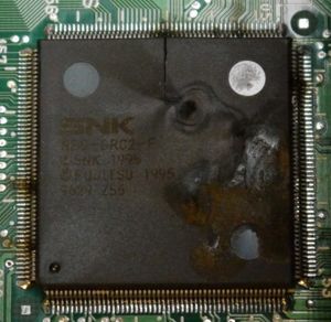
Visual inspection can reveal physically damaged chips. Burnt, deformed or cracked chips are definitely dead.
On NeoGeo systems, burnt chips are often the sign that the 5V rail went way higher than 5V, probably because of a cab or supergun power supply failure, 12V short, or wrong a connection of the JAMMA connector. Several chips are usually killed in that case, but all won't show visible damage.
Some chips may have survived on the board. May have.
Internal damage
Internal chip damage is more common, and can't be detected visually. Voltage spikes or shorts may cause irreversible damage to the die, resulting in floating or "stuck" pins.
That's why some pins of multi-purpose SNK chips like NEO-I0 may still function, but others may be dead, floating. Some SNK chips can be saved if they're mostly functioning. The dead pins can be cut off and replaced with discreet logic chips with a bit of courage.
RAM having unexplainable behavior are certainly internally damaged and need to be replaced. Multiple RAM chips may have been killed by a "long" voltage spike. RAM chips also tend to die one after the other on cabs which have their PSU dying, or with a badly adjusted 5V output.
MVS
Backup RAM error
Typical message looks like: Backup RAM error: Address 00D00000; Written 5555; Read 0000.
The last part is the most usefull: Written XXXX Read YYZZ
The YYZZ represent upper and lower bytes - each one handled by different SRAM IC: YY is upper RAM, ZZ is lower RAM.
The value can help you to know which line/trace cause problem.
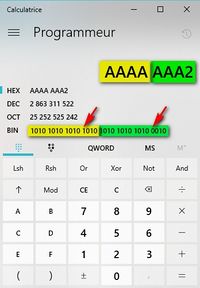
For example writting AAAA and reading AAA2 means the 4th data line of lower RAM causes problem.

Video RAM error
- Address between $0000 and $7FFF: Check CXK58257 VRAM chips next to GPUs (see RAM_chip).
- Address between $8000 and $86FF: Check CXK5814 VRAM chips (see RAM_chip).
- Read high byte is different: check RAM chip with highest number.
- Read low byte is different: check RAM chip with lowest number.
- Read byte stuck to $FF (bad /OE ?), only a few bits different (traces cut ?), random address (floating /OE, /CE ?)
No sound
- Backup RAM corrupt, SOUND_STOP ($D00046) is non-zero. Clear Backup RAM.
- YM2610 has no clock, bad control signals (/CS mainly), or dead.
- YM3016 has cut traces to YM2610, or dead.
- Low sound level: recap audio section.
- Power amp is fried.
- Unplugged or faulty NEO-CDD board.
- Dead op-amps.
Z80 error
Can be caused by bad components / continuity with the following:
- Z80 <-> SM1
- Z80 <-> RAM
Second generation specific (todo: get pin numbers in a nice table)
- Z80 <-> NEO-D0 (NMI,A2-A4,IORQ)
- Z80 <-> NEO-C1 (Z80 D0-D7)
- NEO-D0 <-> NEO-C1 (Z80R,Z80W,Z80CLR,SDW)