LSPC2-A2: Difference between revisions
Jump to navigation
Jump to search
mNo edit summary |
mNo edit summary |
||
| (10 intermediate revisions by the same user not shown) | |||
| Line 1: | Line 1: | ||
{{ChipInfo | |||
|picture=aes_lspc2a2.jpg | |||
|pkg=QFP176 | |||
|manu=fujitsu | |||
|date=1992 ? | |||
|gates= | |||
|used_on={{PCB|NEO-AES3-4 board}} {{PCB|MV1FZS}}... | |||
}} | |||
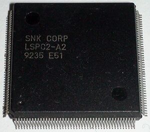
LSPC2-A2 is the second generation Line SPrite Controller, it is only found in cartridge systems. | |||
*Generates | *Generates {{Chipname|S ROM}}, {{Chipname|C ROM}} and {{Chipname|LO}} ROM addresses based on current display line and [[VRAM]] content | ||
*Sync output | *Sync output | ||
*{{Chipname|NEO-B1}} control | |||
*68k IRQs | *68k IRQs | ||
*68k VRAM access | *68k VRAM access arbitration | ||
LSPC-A0 chips can be | First generation {{Chipname|LSPC-A0}} chips can be found in earlier systems. | ||
=Graphics= | |||
Two separate | Two separate busses run in parallel to fetch data from the two VRAM zones. Each bus connects to a pair of 8-bit RAM chips. | ||
*VRAM 0000 | *VRAM $0000~$7FFF - 2x 62256/43256 | ||
*VRAM 8000 | *VRAM $8000~$87FF - 2x 5814/5863/6116 | ||
The LSPC arbitrates all VRAM access and allows for 68k access at any time during rendering without display glitches. | The LSPC arbitrates all VRAM access and allows for {{Chipname|68k}} access at any time during rendering without display glitches if they aren't made too fast. See [[VRAM]] for timing requirements. | ||
It shares | It shares the 24-bit [[P bus]] (P0~P23) with NEO-B1 and the on-board [[L0 ROM]], which goes out to the [[Pinouts#Cartridges|CHA connector]] on the cart slot for addressing {{Chipname|S ROM}}s and {{Chipname|C ROM}}s. | ||
= | =IRQs= | ||
All 3 [[68k interrupts]] are generated by this chip. | All 3 possible [[68k interrupts]] are generated by this chip. | ||
=Pinout= | |||
{{Pinout|LSPC2-A2|640}} | |||
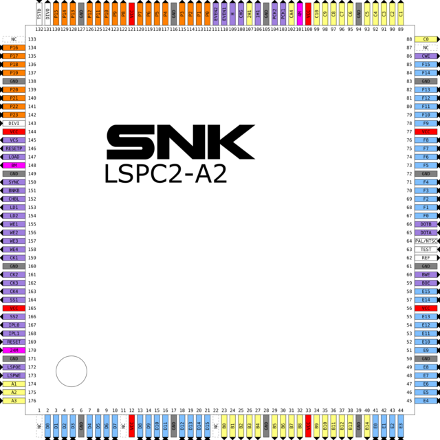
*A1~A3: 68k address bus | |||
*D0~D15: 68k data bus | |||
*A1~A3: | */LSPOE, /LSPWE: Decoded chip read/write | ||
*D0~D15: | *B0~B14: Low VRAM address bus | ||
*B0~B14: VRAM | *E0~E15: Low VRAM data bus | ||
*E0~E15: VRAM | */BOE, /BWE: Low VRAM read/write | ||
*C0~C10: Fast VRAM address bus | |||
*/CWE: Fast VRAM write enable | |||
*F0~F15: Fast VRAM data bus | |||
*/BOE,/BWE: VRAM | *P0~P23: Multiplexed [[P bus]] | ||
*/CWE: VRAM | *1H1: [[Clock]] used by NEO-B1 | ||
* | |||
* | |||
*1H1: | |||
*2H1: S ROM A3 | *2H1: S ROM A3 | ||
*24M: 24MHz clock input from | *24M: 24MHz clock input from {{Chipname|NEO-D0}} | ||
*4M: 4MHz clock output to | *8M: 8MHz clock output to the {{Chipname|YM2610}} | ||
* | *4M: 4MHz clock output to the {{Chipname|Z80}} | ||
*DIVI | *CA4: C ROM A4 | ||
* | *DIVI, DIVO, REF, TSTD: Independant frequency division circuit used by the [[video PLL]] | ||
* | *EVEN1, EVEN2, H, LOAD: C ROM serializer control, see {{Chipname|NEO-ZMC2}} | ||
*DOTA, DOTB: Pixel opacity inputs from NEO-ZMC2 | |||
*IP0 | *IP0, IP1: 68k interrupt lines | ||
*PK1: Clock to latch C ROM address from | *PK1: Clock to latch C ROM address from P bus | ||
*PK2: Clock to latch S ROM address from | *PK2: Clock to latch S ROM address from P bus | ||
* | *RESETP: Reset pulse output | ||
*SYNC: Video sync signal output | |||
*TST: Enable test mode, uses D0~D10 (always tied to ground) | |||
*VCS: L0 ROM output enable | |||
*WE1~WE4: Synchronous write enable signals for NEO-B1 | |||
*SYNC: | *CK1~CK4: Clocks for rendering and output for NEO-B1 | ||
*TST: | *SS1, SS2: NEO-B1 control | ||
*BNKB: Video blanking (for V-blank) | |||
*VCS: | *CHBL: Video blanking (for H-blank, sent to NEO-B1) | ||
*WE1~WE4 | *PAL/NTSC: Video mode selection, latched during reset | ||
* | |||
* | |||
[[Category:Chips]] | [[Category:Chips]] | ||
Latest revision as of 01:10, 8 July 2018

| |
| Package | QFP176 |
| Manufacturer | |
| First use | 1992 ? |
| Used on | NEO-AES3-4 board MV1FZS... |
LSPC2-A2 is the second generation Line SPrite Controller, it is only found in cartridge systems.
- Generates S ROM, C ROM and LO ROM addresses based on current display line and VRAM content
- Sync output
- NEO-B1 control
- 68k IRQs
- 68k VRAM access arbitration
First generation LSPC-A0 chips can be found in earlier systems.
Graphics
Two separate busses run in parallel to fetch data from the two VRAM zones. Each bus connects to a pair of 8-bit RAM chips.
- VRAM $0000~$7FFF - 2x 62256/43256
- VRAM $8000~$87FF - 2x 5814/5863/6116
The LSPC arbitrates all VRAM access and allows for 68k access at any time during rendering without display glitches if they aren't made too fast. See VRAM for timing requirements.
It shares the 24-bit P bus (P0~P23) with NEO-B1 and the on-board L0 ROM, which goes out to the CHA connector on the cart slot for addressing S ROMs and C ROMs.
IRQs
All 3 possible 68k interrupts are generated by this chip.
Pinout
- A1~A3: 68k address bus
- D0~D15: 68k data bus
- /LSPOE, /LSPWE: Decoded chip read/write
- B0~B14: Low VRAM address bus
- E0~E15: Low VRAM data bus
- /BOE, /BWE: Low VRAM read/write
- C0~C10: Fast VRAM address bus
- /CWE: Fast VRAM write enable
- F0~F15: Fast VRAM data bus
- P0~P23: Multiplexed P bus
- 1H1: Clock used by NEO-B1
- 2H1: S ROM A3
- 24M: 24MHz clock input from NEO-D0
- 8M: 8MHz clock output to the YM2610
- 4M: 4MHz clock output to the Z80
- CA4: C ROM A4
- DIVI, DIVO, REF, TSTD: Independant frequency division circuit used by the video PLL
- EVEN1, EVEN2, H, LOAD: C ROM serializer control, see NEO-ZMC2
- DOTA, DOTB: Pixel opacity inputs from NEO-ZMC2
- IP0, IP1: 68k interrupt lines
- PK1: Clock to latch C ROM address from P bus
- PK2: Clock to latch S ROM address from P bus
- RESETP: Reset pulse output
- SYNC: Video sync signal output
- TST: Enable test mode, uses D0~D10 (always tied to ground)
- VCS: L0 ROM output enable
- WE1~WE4: Synchronous write enable signals for NEO-B1
- CK1~CK4: Clocks for rendering and output for NEO-B1
- SS1, SS2: NEO-B1 control
- BNKB: Video blanking (for V-blank)
- CHBL: Video blanking (for H-blank, sent to NEO-B1)
- PAL/NTSC: Video mode selection, latched during reset
