|
|
| Line 1: |
Line 1: |
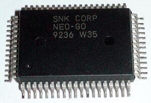
| [[File:Aes_g0.jpg|right|thumb]]
| | {{ChipInfo |
| | |picture=Aes_g0.jpg |
| | |pkg=QFP64R |
| | |manu=fujitsu |
| | |date=1992 ? |
| | |gates= |
| | |used_on={{PCB|MV2B}} ... |
| | }} |
|
| |
|
| Quadruple 245 with OR and AND gates. Predecessor of [[NEO-BUF]]. | | Quadruple 245 with additional OR and AND gates. Predecessor of {{Chipname|NEO-BUF}}. |
|
| |
|
| =Internal logic= | | =Internal logic= |
Revision as of 01:24, 12 October 2016

|
| Package
|
QFP64R
|
| Manufacturer
|

|
| First use
|
1992 ?
|
| Used on
|
MV2B ...
|
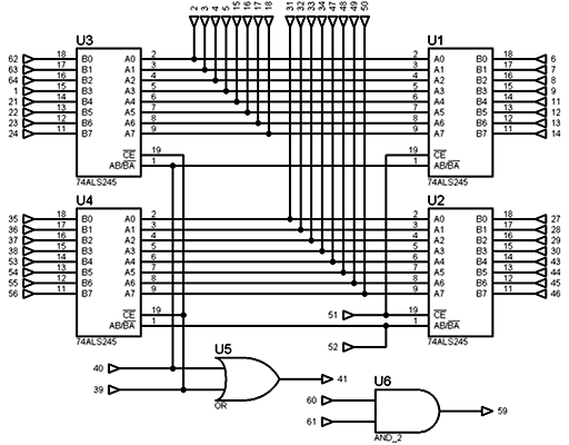
Quadruple 245 with additional OR and AND gates. Predecessor of NEO-BUF.
Internal logic
|

|
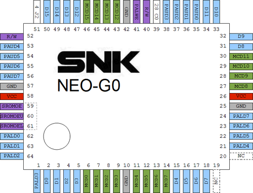
- Pin 51 is enable for MCD0~MCD15
- Pin 39 is enable for PALD0~PALD15
- Pin 40 is direction select for D0~D7
- Pin 52 is direction select for D8~D15
|
AES pinout
Palette RAM and memory card access. Palette RAM /WE and P1 ROM /OE generation.
|
File:Neo-g0 aes pinout.png
OpenOffice Draw file: File:Neo-g0 aes.odg
|
- D0~D15: 68k data bus
- PALD0~PALD7: Lower palette RAM data bus
- PAUD0~PAUD7: Upper palette RAM data bus
- MCD0~MCD15: Memory card data bus
- PAL: Palette RAM address decode from NEO-C1
- R/W: R/W from 68k
- PALWE: Palette RAM /WE, output made from PAL OR R/W
- ROMOEL, ROMOEU: from PRO-C0
- ROMOE: Cartridge P ROM /OE, output made from ROMOEU AND ROMOEL
|
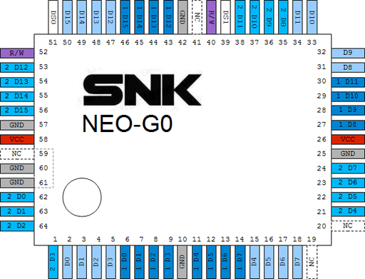
MV2B @ J4 pinout
68k data bus access for both slots.
|

OpenOffice Draw file: File:Neo-g0 mv2b J4.odg
|
- D0~D15: 68k data bus
- 1D0~1D15: Slot 1 68k data bus
- 2D0~2D15: Slot 2 68k data bus
- DS0,DS1: Slot 68k data enables from NEO-I0
- R/W: R/W from 68k
|
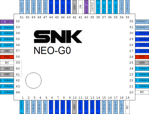
MV2B @ J12 pinout
ADPCM buses access for both slots.
|

OpenOffice Draw file: File:Neo-g0 mv2b J12.odg
|
- SDRAD0~SDRAD7: ADPCM-A data bus from YM2610
- 1SDRAD0~1SDRAD7: ADPCM-A data bus for slot 1
- 2SDRAD0~2SDRAD7: ADPCM-A data bus for slot 2
- SDPAD0~SDPAD7: ADPCM-B data bus from YM2610
- 1SDPAD0~1SDPAD7: ADPCM-B data bus for slot 1
- 2SDPAD0~2SDPAD7: ADPCM-B data bus for slot 2
- 10 AS04: negated /ROE from YM2610
- 12 AS04: negated /POE from YM2610
- SLOT0, SLOT1: enables from NEO-F0
|
MV2B @ C7 pinout
Palette RAM and memory card access. Palette RAM /WE and System ROM /OE generation.
|

OpenOffice Draw file: File:Neo-g0 mv2b C7.odg
|
Very similar connections with the one used in the AES.
- D0~D15: 68k data bus
- PALD0~PALD7: Lower palette RAM data bus
- PAUD0~PAUD7: Upper palette RAM data bus
- MCD0~MCD15: Memory card data bus
- 28 C0 (PAL ?):Palette RAM address decode from PRO-C0
- R/W: R/W from 68k
- PALWE: Palette RAM /WE, output made from PAL OR R/W
- SROMOEL, SROMOEU: from PRO-C0, System ROM byte /OE
- ROMOE: System ROM ROM /OE, output made from SROMOEU AND SROMOEL
|
