NEO-G0: Difference between revisions
Jump to navigation
Jump to search
mNo edit summary |
m (BIOS -> system ROM) |
||
| Line 89: | Line 89: | ||
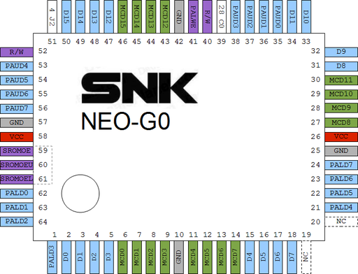
=MV2B @ C7 pinout= | =MV2B @ C7 pinout= | ||
Palette RAM and memory card access. Palette RAM /WE and | Palette RAM and memory card access. Palette RAM /WE and System ROM /OE generation. | ||
{| | {| | ||
| Line 107: | Line 107: | ||
*PALWE: Palette RAM /WE, output made from PAL OR R/W | *PALWE: Palette RAM /WE, output made from PAL OR R/W | ||
*SROMOEL, SROMOEU: from PRO-C0, | *SROMOEL, SROMOEU: from PRO-C0, System ROM byte /OE | ||
*ROMOE: [[ | *ROMOE: [[System ROM]] ROM /OE, output made from SROMOEU AND SROMOEL | ||
|} | |} | ||
Revision as of 09:23, 23 November 2015
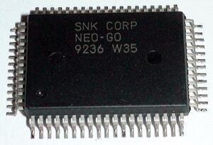
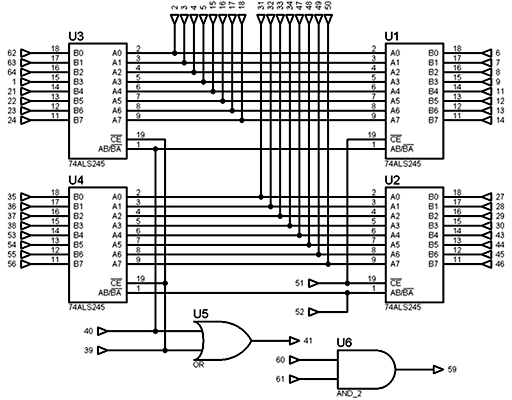
Quadruple 245 with OR and AND gates. Predecessor of NEO-BUF.
Internal logic
|
AES pinout
Palette RAM and memory card access. Palette RAM /WE and P1 ROM /OE generation.
|
OpenOffice Draw file: File:Neo-g0 aes.odg |
|
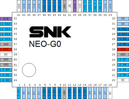
MV2B @ J4 pinout
68k data bus access for both slots.
|
OpenOffice Draw file: File:Neo-g0 mv2b J4.odg |
|
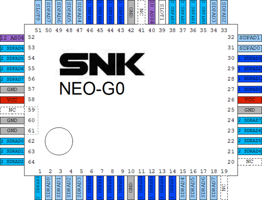
MV2B @ J12 pinout
ADPCM buses access for both slots.
|
OpenOffice Draw file: File:Neo-g0 mv2b J12.odg |
|
MV2B @ C7 pinout
Palette RAM and memory card access. Palette RAM /WE and System ROM /OE generation.
|
OpenOffice Draw file: File:Neo-g0 mv2b C7.odg |
Very similar connections with the one used in the AES.
|
