NEO-C1: Difference between revisions
Jump to navigation
Jump to search
No edit summary |
mNo edit summary |
||
| Line 8: | Line 8: | ||
}} | }} | ||
The NEO-C1 is a multi-purpose keystone chip used for address decoding, inter-CPU communications, [[wait cycle]] generation, and [[joypad|player input]]s on systems based on the 2nd generation chipset. | |||
It maps itself to [[68k]] even byte accesses. | |||
=Pinout= | =Pinout= | ||
{{Pinout|NEO-C1|900}} | {{Pinout|NEO-C1|900}} | ||
=Internal schematics= | |||
https://github.com/furrtek/SiliconRE/tree/master/SNK/NEO-C1 | |||
=Signals= | =Signals= | ||
| Line 55: | Line 59: | ||
*A22I~A23I: [[NEO-E0]] address input | *A22I~A23I: [[NEO-E0]] address input | ||
*D8~D15: 68k data bus | *D8~D15: 68k data bus | ||
*R/W,UDS,LDS,AS,DTACK: 68k bus control signals | *R/W, UDS, LDS, AS, DTACK: 68k bus control signals | ||
*68KCLK: 12MHz 68k clock | *68KCLK: 12MHz 68k clock | ||
*ROMWAIT,PWAIT0,PWAIT1,PDTACK: signals from cart PROG board to configure | *ROMWAIT, PWAIT0, PWAIT1, PDTACK: signals from cart PROG board to configure [[wait cycle]]s. | ||
==Decoded signals== | ==Decoded signals== | ||
| Line 63: | Line 67: | ||
The following output and write enables have an upper(U)/lower(L) byte enable signal based on /UDS and /LDS from the 68k. | The following output and write enables have an upper(U)/lower(L) byte enable signal based on /UDS and /LDS from the 68k. | ||
*ROMOEU,ROMOEL: $000000-$0FFFFF read, 68k program ROM on cart | *ROMOEU, ROMOEL: $000000-$0FFFFF read, 68k program ROM on cart / vector table | ||
*WRU,WRL,WWU,WWL: $100000-$1FFFFF read/write | *WRU, WRL, WWU, WWL: $100000-$1FFFFF read/write [[68k user RAM]] | ||
*PORTOEU,PORTOEL,PORTWEU,PORTWEL: $200000-$2FFFFF read/write, | *PORTOEU, PORTOEL, PORTWEU, PORTWEL: $200000-$2FFFFF read/write, 68k program ROM and/or security chips on cart | ||
*SROMOEU,SROMOEL: $C00000-$CFFFFF read | *SROMOEU, SROMOEL: $C00000-$CFFFFF read [[system ROM]] | ||
*SRAMOEU,SRAMOEL,SRAMWEU,SRAMWEL: $D00000-$DFFFFF read/write | *SRAMOEU, SRAMOEL, SRAMWEU, SRAMWEL: $D00000-$DFFFFF read/write [[battery-backed RAM]] | ||
When A23I A22I A21 A20 = 1100 and RW = 1, either SROMOEU and SROMOEL should be low depending on UDS and LDS. | |||
The following are expected to be word accessed, byte writes and reads are ignored or do not work as expected. | The following are expected to be word accessed, byte writes and reads are ignored or do not work as expected. | ||
*CRDO,CRDW: $800000-$BFFFFF read/write | *CRDO, CRDW: $800000-$BFFFFF read/write [[memory card]] | ||
*CRDC: Memory card select | *CRDC: Memory card select | ||
*LSPOE,LSPWE: $3C0000-$3DFFFF read/write | *LSPOE, LSPWE: $3C0000-$3DFFFF read/write [[LSPC2-A2]] | ||
*PAL: $400000-$7FFFFF | *PAL: $400000-$7FFFFF read/write [[palette RAM]] | ||
==Z80 I/O== | ==Z80 I/O== | ||
*SDD0~SDD7: [[Z80]] data bus used for [[68k/Z80 communication]] | *SDD0~SDD7: [[Z80]] data bus used for [[68k/Z80 communication]] | ||
*SDZ80R,SDZ80W: read / write signals for Z80 communication | *SDZ80R, SDZ80W: read / write signals for Z80 communication | ||
*SDW: signals that 68k has written a byte to Z80 port, will make [[NEO-D0]] generate interrupt if enabled | *SDW: signals that 68k has written a byte to Z80 port, will make [[NEO-D0]] generate an interrupt if enabled | ||
*SDZ80CLR: | *SDZ80CLR: reset stored byte | ||
[[Category:Chips]] | [[Category:Chips]] | ||
Revision as of 02:38, 29 November 2024

| |
| Package | QFP100R |
| Manufacturer | |
| First use | 1992 ? |
| Used on | NEO-AES3-4 board... |
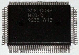
The NEO-C1 is a multi-purpose keystone chip used for address decoding, inter-CPU communications, wait cycle generation, and player inputs on systems based on the 2nd generation chipset.
It maps itself to 68k even byte accesses.
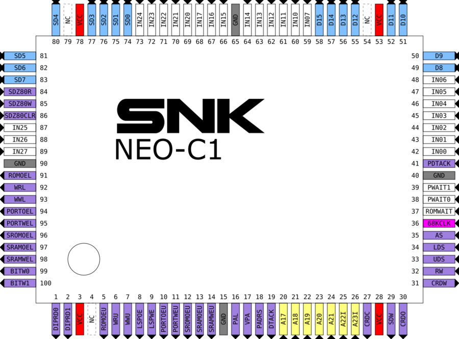
Pinout
Internal schematics
https://github.com/furrtek/SiliconRE/tree/master/SNK/NEO-C1
Signals
Inputs
- IN00: Up P1
- IN01: Down P1
- IN02: Left P1
- IN03: Right P1
- IN04: A P1
- IN05: B P1
- IN06: C P1
- IN07: D P1
- IN10: Up P2
- IN11: Down P2
- IN12: Left P2
- IN13: Right P2
- IN14: A P2
- IN15: B P2
- IN16: C P2
- IN17: D P2
- IN20: Start P1
- IN21: Select P1
- IN22: Start P2
- IN23: Select P2
- IN24: Memory card inserted
- IN25: Memory card inserted
- IN26: Memory card write protect
- IN27: System type (home/arcade)
68k
- A17~A21: 68k address bus
- A22I~A23I: NEO-E0 address input
- D8~D15: 68k data bus
- R/W, UDS, LDS, AS, DTACK: 68k bus control signals
- 68KCLK: 12MHz 68k clock
- ROMWAIT, PWAIT0, PWAIT1, PDTACK: signals from cart PROG board to configure wait cycles.
Decoded signals
The following output and write enables have an upper(U)/lower(L) byte enable signal based on /UDS and /LDS from the 68k.
- ROMOEU, ROMOEL: $000000-$0FFFFF read, 68k program ROM on cart / vector table
- WRU, WRL, WWU, WWL: $100000-$1FFFFF read/write 68k user RAM
- PORTOEU, PORTOEL, PORTWEU, PORTWEL: $200000-$2FFFFF read/write, 68k program ROM and/or security chips on cart
- SROMOEU, SROMOEL: $C00000-$CFFFFF read system ROM
- SRAMOEU, SRAMOEL, SRAMWEU, SRAMWEL: $D00000-$DFFFFF read/write battery-backed RAM
When A23I A22I A21 A20 = 1100 and RW = 1, either SROMOEU and SROMOEL should be low depending on UDS and LDS.
The following are expected to be word accessed, byte writes and reads are ignored or do not work as expected.
- CRDO, CRDW: $800000-$BFFFFF read/write memory card
- CRDC: Memory card select
- LSPOE, LSPWE: $3C0000-$3DFFFF read/write LSPC2-A2
- PAL: $400000-$7FFFFF read/write palette RAM
Z80 I/O
- SDD0~SDD7: Z80 data bus used for 68k/Z80 communication
- SDZ80R, SDZ80W: read / write signals for Z80 communication
- SDW: signals that 68k has written a byte to Z80 port, will make NEO-D0 generate an interrupt if enabled
- SDZ80CLR: reset stored byte
