NEO-I0: Difference between revisions
Jump to navigation
Jump to search
mNo edit summary |
No edit summary |
||
| (11 intermediate revisions by 2 users not shown) | |||
| Line 1: | Line 1: | ||
{{ChipInfo | |||
|picture=neo-i0.jpg | |||
|pkg=QFP64R | |||
|manu=fujitsu | |||
|date=1990 ? | |||
|gates= | |||
|used_on={{PCB|MV2B}} {{PCB|MV1-1}} ... | |||
}} | |||
MVS specific chip that does a bunch of unrelated things. | MVS specific chip that does a bunch of unrelated things. | ||
*[[S ROM]] address latch for [[SFIX]], same as S ROM portion of | * [[S ROM]] 16bit address latch for the [[SFIX ROM]], same as S ROM portion of {{Chipname|NEO-273}} | ||
*[[SM1]] /CS output when Z80 is reading from ROM and | * [[SM1]] /CS output when {{Chipname|Z80}} is reading from ROM and onboard ROMs are enabled | ||
* | * {{Sig|ROMOE|ROMOE}} output for cartridge(s) [[PROG board]] | ||
*Video sync | * Video sync inversion (or not) to [[JAMMA_connector_pinout|JAMMA connector]] | ||
*Coin counter and coin lockout | * [[Coin counter]] and [[coin lockout]] outputs | ||
=Pinout= | =Pinout= | ||
{{Pinout|NEO-I0|640px}} | |||
*A1~A3,A7: {{Chipname|68k}} address bus | |||
* | *P0~P15: [[P bus]] | ||
*SM1CS(ORO0) | *Q01~Q18: [[SFIX ROM]] address lines | ||
*SYNCOUT = SYNCIN XOR SYNCREV ? | *SM1CS(ORO0): [[SM1]] ROM chip select, made from SYSTEM(ORI0) OR SDROM(ORI1) | ||
*Q21,Q22:METER1,METER2 | *SYNCOUT = SYNCIN XOR SYNCREV (SYNCREV always tied to ground ?) | ||
*Q23,Q24:LOCK1,LOCK2 | *Q21, Q22: METER1, METER2 | ||
*Q23, Q24: LOCK1, LOCK2 | |||
*DS0, DS1: Data select for 2-slot systems made from SLOT0, SLOT1, PORTADRS and ROMOE, goes to a {{Chipname|NEO-G0}} | |||
*COUNTOUT: Address decode from {{Chipname|NEO-F0}} | |||
[[Category:Chips]] | [[Category:Chips]] | ||
Latest revision as of 11:47, 18 November 2018

| |
| Package | QFP64R |
| Manufacturer | |
| First use | 1990 ? |
| Used on | MV2B MV1-1 ... |
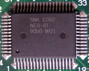
MVS specific chip that does a bunch of unrelated things.
- S ROM 16bit address latch for the SFIX ROM, same as S ROM portion of NEO-273
- SM1 /CS output when Z80 is reading from ROM and onboard ROMs are enabled
- ROMOE output for cartridge(s) PROG board
- Video sync inversion (or not) to JAMMA connector
- Coin counter and coin lockout outputs
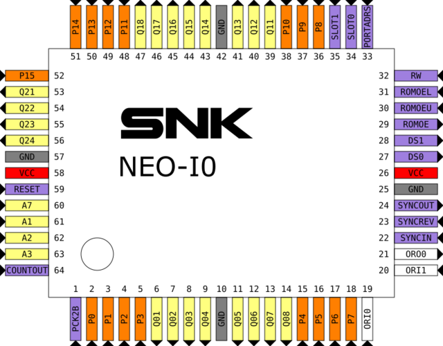
Pinout
- A1~A3,A7: 68k address bus
- P0~P15: P bus
- Q01~Q18: SFIX ROM address lines
- SM1CS(ORO0): SM1 ROM chip select, made from SYSTEM(ORI0) OR SDROM(ORI1)
- SYNCOUT = SYNCIN XOR SYNCREV (SYNCREV always tied to ground ?)
- Q21, Q22: METER1, METER2
- Q23, Q24: LOCK1, LOCK2
- DS0, DS1: Data select for 2-slot systems made from SLOT0, SLOT1, PORTADRS and ROMOE, goes to a NEO-G0
- COUNTOUT: Address decode from NEO-F0
