Schematics: Difference between revisions
Jump to navigation
Jump to search
mNo edit summary |
m (BIOS -> system ROM) |
||
| Line 26: | Line 26: | ||
*[[68k user RAM|68k RAM]] | *[[68k user RAM|68k RAM]] | ||
*[[Battery-backed RAM]] | *[[Battery-backed RAM]] | ||
*[[ | *[[System ROM|SP1]] | ||
*[[NEO-C1]] | *[[NEO-C1]] | ||
*[[joypad]] ports | *[[joypad]] ports | ||
Revision as of 06:39, 28 October 2015
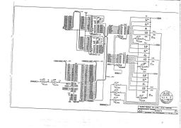
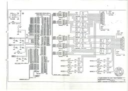
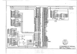
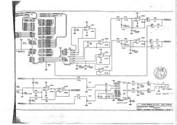
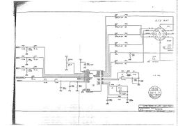
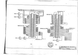
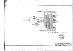
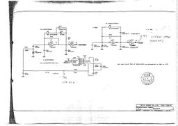
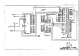
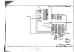
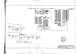
AES
Big thanks to Wolfsoft and ArcadeTV for the scans.
|
|
|
MVS
Beware ! There's an error on page 9 (cartridge edge connections): ROMOE/4MB are swapped. ROMOE should be on pin 33 bottom, and 4MB is on pin 34 bottom.
Page 1
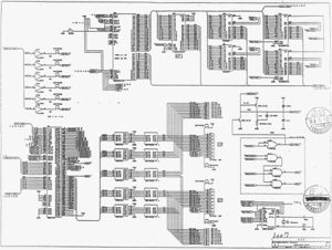
Page 2
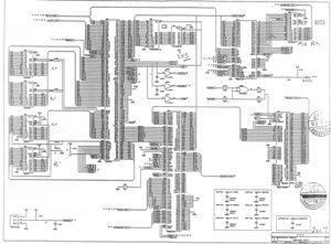
Page 3
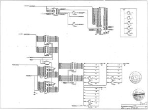
- System register latch
- NEO-E0
- palette RAM
- video DAC
Page 4
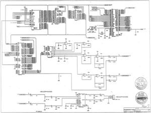
Page 5
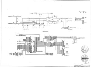
- speaker amp
- NEO-F0
- DIP switches
- cab outputs
Page 6
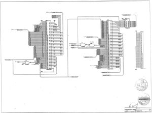
Daughterboard connections (0%)
Page 7
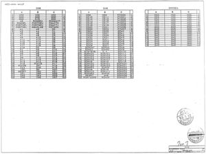
Page 8
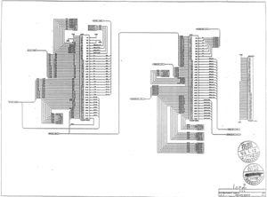
Daughterboard connections (0%)
Page 9
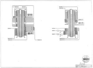
Cartridge connections (0%)
Vectorized version: Link to last SVG file:
