NEO-AES board: Difference between revisions
Jump to navigation
Jump to search
m (PCB map) |
m (Voltage protection circuit) |
||
| Line 1: | Line 1: | ||
First | First known version of the AES board, made (and maybe assembled) by NEC. Uses the first generation chipset {{Chipname|PRO-B0}}, {{Chipname|PRO-C0}}, {{Chipname|LSPC-A0}}. | ||
In | In later use of this board version, a [[video PLL|video cleaner]] board was added. | ||
Some consoles also have | Some consoles also have a metal shield connected to ground. | ||
=Voltage protection= | |||
The voltage protection circuit changed during the production of the board: | |||
* The first boards simply had no voltage protection. Meaning that using a higher than [[power requirements|5V power supply]] would fry everything. | |||
* Later on, components were added to dump excessive voltage as heat (see below). | |||
* Even later, the [[NEO-POWER-0]] board was added as a factory mod to allow the safe use of 9V power supplies. | |||
The voltage protection circuit starts operating as soon as the input voltage goes above 5.4V. If used with a 9V power supply for an extended period of time, it may fail due to excessive heat. Q2 and/or D1 may need to be replaced. | |||
[[File:Neo-aes_power.png|400px]] | |||
[[File:Neo-aes_power2.png|400px]] | |||
=Board map= | =Board map= | ||
| Line 34: | Line 46: | ||
* 8E: Fast [[VRAM]] chips | * 8E: Fast [[VRAM]] chips | ||
* 8OPQR: [[Memory card]] slot | * 8OPQR: [[Memory card]] slot | ||
* 9C: Voltage protection circuit | |||
* 9EF: [[Joypad]] input [[CRE401|filters]] | * 9EF: [[Joypad]] input [[CRE401|filters]] | ||
* 9HIJK: Analog sound circuit | * 9HIJK: Analog sound circuit | ||
| Line 44: | Line 57: | ||
[[Category:Cartridge systems]] | [[Category:Cartridge systems]] | ||
[[Category:Repairs]] | |||
Latest revision as of 01:48, 28 August 2019
First known version of the AES board, made (and maybe assembled) by NEC. Uses the first generation chipset PRO-B0, PRO-C0, LSPC-A0.
In later use of this board version, a video cleaner board was added.
Some consoles also have a metal shield connected to ground.
Voltage protection
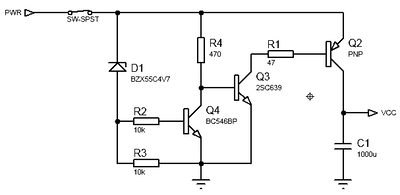
The voltage protection circuit changed during the production of the board:
- The first boards simply had no voltage protection. Meaning that using a higher than 5V power supply would fry everything.
- Later on, components were added to dump excessive voltage as heat (see below).
- Even later, the NEO-POWER-0 board was added as a factory mod to allow the safe use of 9V power supplies.
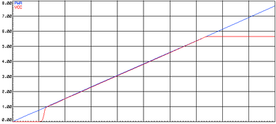
The voltage protection circuit starts operating as soon as the input voltage goes above 5.4V. If used with a 9V power supply for an extended period of time, it may fail due to excessive heat. Q2 and/or D1 may need to be replaced.
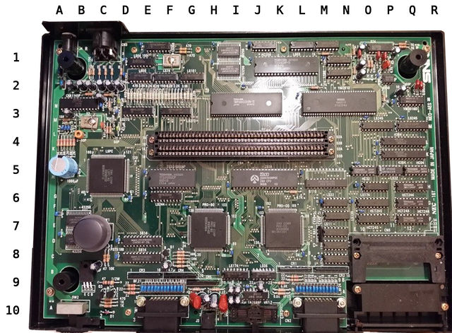
Board map

- 1A: Power supply barrel jack connector
- 1C: Audio/video output DIN connector
- 1F: Main clock circuit
- 1I: 68k user RAM chips
- 1J: System latch
- 1KL: System ROM
- 1OPQ: Analog sound circuit
- 2EF: Video DAC
- 2Q: YM3016
- 3B: Video encoder and color burst oscillator
- 3EF: Palette RAM latches
- 3HIJK: 68k CPU
- 3LMNO: YM2610 soundchip
- 4F~M: Cartridge slot
- 4PQ: Palette RAM chips
- 5CD: LSPC-A0
- 5FG: L0 ROM
- 5IJK: Z80 CPU
- 6M: Z80 RAM
- 7B: Slow VRAM chips
- 7C: Reset button
- 7H: PRO-B0
- 7K: PRO-C0
- 8E: Fast VRAM chips
- 8OPQR: Memory card slot
- 9C: Voltage protection circuit
- 9EF: Joypad input filters
- 9HIJK: Analog sound circuit
- 9LM: More joypad input filters
- 10B: Power switch
- 10F: P1 connector
- 10H: Headphone 3.5mm stereo jack connector
- 10J: Headphone volume slider
- 10M: P2 connector

