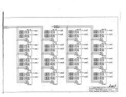
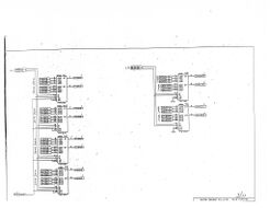
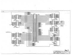
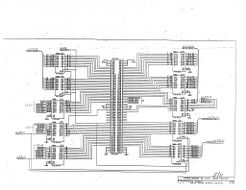
Schematics: Difference between revisions
m (Furrtek moved page MVS schematics to Schematics) |
(fix image link) |
||
| (16 intermediate revisions by 6 users not shown) | |||
| Line 1: | Line 1: | ||
__TOC__ | |||
=AES (Home system)= | |||
Big thanks to Wolfsoft and ArcadeTV for the scans. | |||
* On page 6: There are two resistors in the bottom left corner that can't be seen due the page fold. | |||
* The R48 4.7k is connected to VCC and R49 4.7k is connected to GND. | |||
* Both resistors are connected to pin3 of U31A. | |||
<gallery widths=300px heights=190px perrow=4> | |||
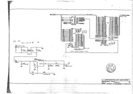
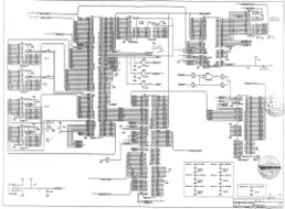
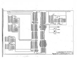
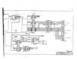
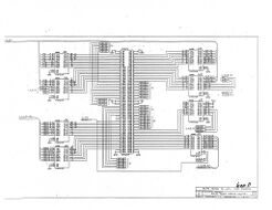
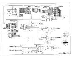
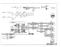
File:Neogeo_aes_schematics_pal_2-page-001.jpg|'''Page 1''':{{Chipname|68k}} [[68k user RAM]] {{Chipname|NEO-C1}} | |||
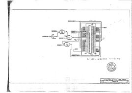
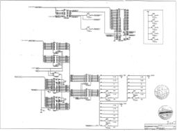
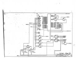
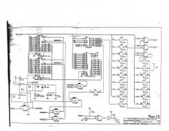
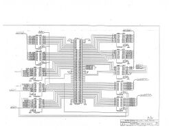
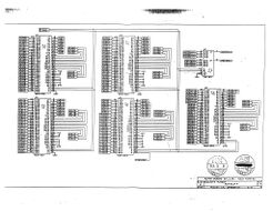
File:Neogeo_aes_schematics_pal_2-page-002.jpg|'''Page 2''':{{Chipname|NEO-G0}} [[Palette RAM]] [[Video DAC]] | |||
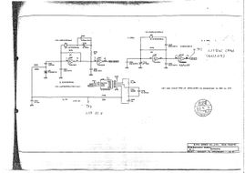
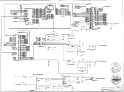
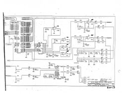
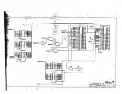
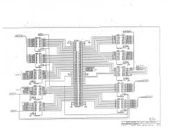
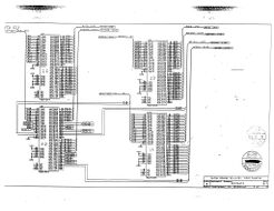
File:Neogeo_aes_schematics_pal_2-page-003.jpg|'''Page 3''':{{Chipname|NEO-B1}} [[Reset generator]] [[Joypad]] ports | |||
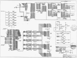
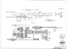
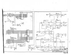
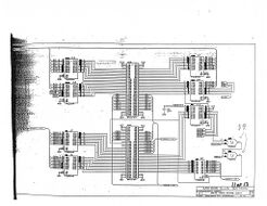
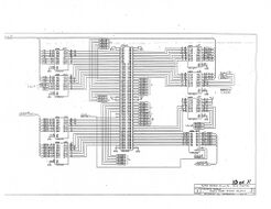
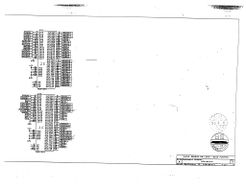
File:Neogeo_aes_schematics_pal_2-page-004.jpg|'''Page 4''':{{Chipname|LSPC2-A2}} [[L0 ROM]] [[VRAM]] | |||
File:NeoGeo Z80-RAM-NEO-DO.png|'''Page 5''':{{Chipname|Z80}} [[Z80 RAM]] {{Chipname|NEO-D0}} [[:File:Neogeo aes schematics pal 2-page-005.jpg|(original scan)]] | |||
File:Neogeo_aes_schematics_pal_2-page-006.jpg|'''Page 6''':{{Chipname|YM2610}} {{Chipname|YM3016}} {{Chipname|NEO-C1}} | |||
File:Neogeo_aes_schematics_pal_2-page-007.jpg|'''Page 7''':[[Video encoder]] | |||
File:Neogeo_aes_schematics_pal_2-page-008.jpg|'''Page 8''':[[Pinouts|cartridge slot]] | |||
File:Neogeo_aes_schematics_pal_2-page-009.jpg|'''Page 9''':[[Memory mapped registers|System latch]] {{Chipname|NEO-E0}} [[Power supply]] | |||
File:Neogeo_aes_schematics_pal_2-page-010.jpg|'''Page 10''':[[Memory card]] | |||
File:Neogeo_aes_schematics_pal_2-page-011.jpg|'''Page 11''':[[Video PLL]] | |||
</gallery> | |||
=MV1F (MVS)= | |||
<span style="color:#FF0000"><B>Beware !</B> There's an error on page 9 (cartridge edge connections): <b>ROMOE/4MB are swapped</B>. ROMOE should be on pin 33 bottom, and 4MB is on pin 34 bottom.</span> | <span style="color:#FF0000"><B>Beware !</B> There's an error on page 9 (cartridge edge connections): <b>ROMOE/4MB are swapped</B>. ROMOE should be on pin 33 bottom, and 4MB is on pin 34 bottom.</span> | ||
= | <gallery widths=300px heights=190px perrow=4> | ||
File:mv1fs-page1.jpg|'''Page 1''':{{Chipname|68k}} [[System ROM]] [[68k user RAM]] [[Battery-backed RAM]] {{Chipname|NEO-C1}} [[Joypad]] ports {{Chipname|UPD4990}} [[Battery circuit]] | |||
File:mv1fs-page2.jpg|'''Page 2''':{{Chipname|LSPC2-A2}} [[VRAM]] {{Chipname|NEO-I0}} {{Chipname|NEO-B1}} {{Chipname|NEO-ZMC2}} [[SFIX ROM]] [[L0 ROM]] | |||
File:mv1fs-page3.jpg|'''Page 3''':{{Chipname|NEO-E0}} [[Memory mapped registers|System latch]] [[Palette RAM]] [[Video DAC]] | |||
File:mv1fs-page4.jpg|'''Page 4''':{{Chipname|Z80}} [[Z80 RAM]] [[SM1]] ROM {{Chipname|NEO-D0}} {{Chipname|YM2610}} {{Chipname|YM3016}} [[Headphone amp]] | |||
File:mv1fs-page5.jpg|'''Page 5''':[[Power amp]] {{Chipname|NEO-F0}} [[DIPs|DIP switches]] [[Cab interface]] | |||
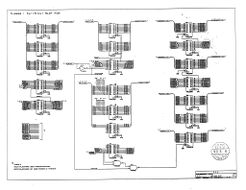
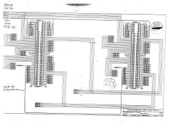
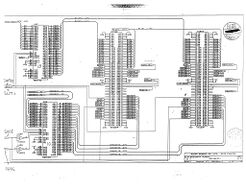
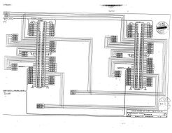
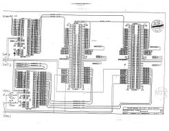
File:mv1fs-page6.jpg|'''Page 6''':Daughterboard connections | |||
File:mv1fs-page7.jpg|'''Page 7''' | |||
File:mv1fs-page8.jpg|'''Page 8''':Daughterboard connections | |||
File:mv1fs-page9.jpg|'''Page 9''':Cartridge connections | |||
</gallery> | |||
=MV4 (MVS)= | |||
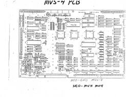
This is the main board of [[MV4|MV4]]. The top board is here after. | |||
PDF file can be found [https://drive.google.com/drive/folders/1QpMv94jbslgKyeiTama89Y3W6AnRzMZS here (GDrive)]. | |||
<gallery widths=300px heights=190px perrow=4> | |||
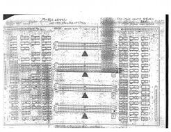
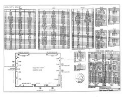
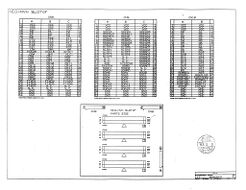
File:MV-4 Schematics 0 PCB.jpg|'''Page 0''': Component placement | |||
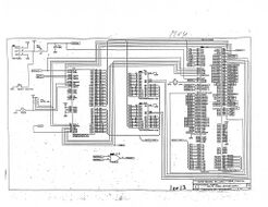
File:MV-4 Schematics 1.jpg|'''Page 1''': todo description | |||
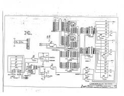
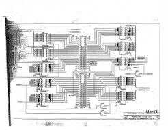
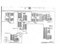
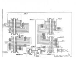
File:MV-4 Schematics 2.jpg|'''Page 2''': todo description | |||
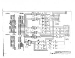
File:MV-4 Schematics 3.jpg|'''Page 3''': todo description | |||
File:MV-4 Schematics 4.jpg|'''Page 4''': todo description | |||
File:MV-4 Schematics 5.jpg|'''Page 5''': todo description | |||
File:MV-4 Schematics 6.jpg|'''Page 6''': todo description | |||
File:MV-4 Schematics 7.jpg|'''Page 7''': todo description | |||
File:MV-4 Schematics 8.jpg|'''Page 8''': todo description | |||
File:MV-4 Schematics 9.jpg|'''Page 9''': todo description | |||
File:MV-4 Schematics 10.jpg|'''Page 10''': todo description | |||
File:MV-4 Schematics 11.jpg|'''Page 11''': todo description | |||
File:MV-4 Schematics 12.jpg|'''Page 12''': todo description | |||
File:MV-4 Schematics 13.jpg|'''Page 13''': todo description | |||
</gallery> | |||
=MV4 Slot4 (MVS)= | |||
This is the top board of [[MV4|MV4]]. | |||
PDF file can be found [https://drive.google.com/drive/folders/1QpMv94jbslgKyeiTama89Y3W6AnRzMZS here (GDrive)]. | |||
=Page 2 | <gallery widths=300px heights=190px perrow=4> | ||
File:MV-4 Schematics slot4 0 PCB.jpg|'''Page 0''': Component placement | |||
File:MV-4 Schematics slot4 1.jpg|'''Page 1''': todo description | |||
File:MV-4 Schematics slot4 2.jpg|'''Page 2''': todo description | |||
File:MV-4 Schematics slot4 3.jpg|'''Page 3''': todo description | |||
File:MV-4 Schematics slot4 4.jpg|'''Page 4''': todo description | |||
File:MV-4 Schematics slot4 5.jpg|'''Page 5''': todo description | |||
File:MV-4 Schematics slot4 6.jpg|'''Page 6''': todo description | |||
File:MV-4 Schematics slot4 7.jpg|'''Page 7''': todo description | |||
File:MV-4 Schematics slot4 8.jpg|'''Page 8''': todo description | |||
File:MV-4 Schematics slot4 9.jpg|'''Page 9''': todo description | |||
File:MV-4 Schematics slot4 10.jpg|'''Page 10''': todo description | |||
File:MV-4 Schematics slot4 11.jpg|'''Page 11''': todo description | |||
</gallery> | |||
= | =MV4F (MVS)= | ||
[[ | This is the main board of [[MV4F|MV4F]]. The top board is here after. | ||
PDF file can be found [https://drive.google.com/drive/folders/1QpMv94jbslgKyeiTama89Y3W6AnRzMZS here (GDrive)]. | |||
= | <gallery widths=300px heights=190px perrow=4> | ||
File:MV-4F Schematics 1.jpg|'''Page 1''': todo description | |||
File:MV-4F Schematics 2.jpg|'''Page 2''': todo description | |||
File:MV-4F Schematics 3.jpg|'''Page 3''': todo description | |||
File:MV-4F Schematics 4.jpg|'''Page 4''': todo description | |||
File:MV-4F Schematics 5.jpg|'''Page 5''': todo description | |||
File:MV-4F Schematics 6.jpg|'''Page 6''': todo description | |||
File:MV-4F Schematics 7.jpg|'''Page 7''': todo description | |||
</gallery> | |||
= | =MV4F Slot4F (MVS)= | ||
[[ | This is the [[SLOT4F|SLOT4F]], alias the top board of [[MV4F|MV4F]]. | ||
PDF file can be found [https://drive.google.com/drive/folders/1QpMv94jbslgKyeiTama89Y3W6AnRzMZS here (GDrive)]. | |||
=Page | <gallery widths=300px heights=190px perrow=4> | ||
File:MV-4F Schematics slot4f 1.jpg|'''Page 1''': todo description | |||
File:MV-4F Schematics slot4f 2.jpg|'''Page 2''': todo description | |||
File:MV-4F Schematics slot4f 3.jpg|'''Page 3''': todo description | |||
File:MV-4F Schematics slot4f 4.jpg|'''Page 4''': todo description | |||
File:MV-4F Schematics slot4f 5.jpg|'''Page 5''': todo description | |||
File:MV-4F Schematics slot4f 6.jpg|'''Page 6''': todo description | |||
File:MV-4F Schematics slot4f 7.jpg|'''Page 7''': todo description | |||
File:MV-4F Schematics slot4f 8.jpg|'''Page 8''': todo description | |||
</gallery> | |||
= | =Peripheral (home/arcade)= | ||
<gallery widths=300px heights=190px perrow4> | |||
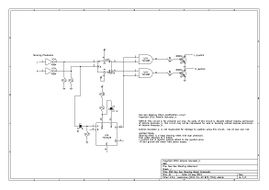
File:Neo Geo Steering Wheel Schematic.jpg|Steering wheel schematic for Thrash Rally. | |||
</gallery> | |||
[[Category:Cartridge systems]] | [[Category:Cartridge systems]] | ||
Latest revision as of 13:18, 23 November 2024
AES (Home system)
Big thanks to Wolfsoft and ArcadeTV for the scans.
- On page 6: There are two resistors in the bottom left corner that can't be seen due the page fold.
- The R48 4.7k is connected to VCC and R49 4.7k is connected to GND.
- Both resistors are connected to pin3 of U31A.
-
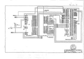
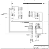
Page 1:68k 68k user RAM NEO-C1
-
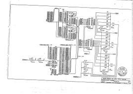
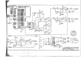
Page 2:NEO-G0 Palette RAM Video DAC
-
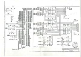
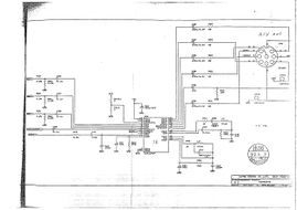
Page 3:NEO-B1 Reset generator Joypad ports
-
Page 5:Z80 Z80 RAM NEO-D0 (original scan)
-
Page 7:Video encoder
-
Page 8:cartridge slot
-
Page 9:System latch NEO-E0 Power supply
-
Page 10:Memory card
-
Page 11:Video PLL
MV1F (MVS)
Beware ! There's an error on page 9 (cartridge edge connections): ROMOE/4MB are swapped. ROMOE should be on pin 33 bottom, and 4MB is on pin 34 bottom.
-
Page 1:68k System ROM 68k user RAM Battery-backed RAM NEO-C1 Joypad ports UPD4990 Battery circuit
-
Page 3:NEO-E0 System latch Palette RAM Video DAC
-
Page 5:Power amp NEO-F0 DIP switches Cab interface
-
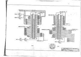
Page 6:Daughterboard connections
-
Page 7
-
Page 8:Daughterboard connections
-
Page 9:Cartridge connections
MV4 (MVS)
This is the main board of MV4. The top board is here after. PDF file can be found here (GDrive).
-
Page 0: Component placement
-
Page 1: todo description
-
Page 2: todo description
-
Page 3: todo description
-
Page 4: todo description
-
Page 5: todo description
-
Page 6: todo description
-
Page 7: todo description
-
Page 8: todo description
-
Page 9: todo description
-
Page 10: todo description
-
Page 11: todo description
-
Page 12: todo description
-
Page 13: todo description
MV4 Slot4 (MVS)
This is the top board of MV4. PDF file can be found here (GDrive).
-
Page 0: Component placement
-
Page 1: todo description
-
Page 2: todo description
-
Page 3: todo description
-
Page 4: todo description
-
Page 5: todo description
-
Page 6: todo description
-
Page 7: todo description
-
Page 8: todo description
-
Page 9: todo description
-
Page 10: todo description
-
Page 11: todo description
MV4F (MVS)
This is the main board of MV4F. The top board is here after. PDF file can be found here (GDrive).
-
Page 1: todo description
-
Page 2: todo description
-
Page 3: todo description
-
Page 4: todo description
-
Page 5: todo description
-
Page 6: todo description
-
Page 7: todo description
MV4F Slot4F (MVS)
This is the SLOT4F, alias the top board of MV4F. PDF file can be found here (GDrive).
-
Page 1: todo description
-
Page 2: todo description
-
Page 3: todo description
-
Page 4: todo description
-
Page 5: todo description
-
Page 6: todo description
-
Page 7: todo description
-
Page 8: todo description
Peripheral (home/arcade)
-
Steering wheel schematic for Thrash Rally.
