NEO-AES3-3 board: Difference between revisions
Jump to navigation
Jump to search
(Added confusing PCB map) |
m (Picture credit) |
||
| Line 2: | Line 2: | ||
=Board map= | =Board map= | ||
Original picture by BIG BEAR. | |||
[[File:neo-aes3-3.jpg|640px|center]] | [[File:neo-aes3-3.jpg|640px|center]] | ||
Revision as of 19:32, 31 October 2016
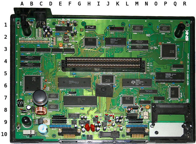
Second (?) version of the AES main board.
Board map
Original picture by BIG BEAR.

- 1A: Power supply barrel jack connector
- 1C: Audio/video output DIN connector
- 1EF: Video encoder
- 1M and 1P: Slow VRAM chips
- 2ABC: Video DAC
- 2F: Color burst oscillator
- 2H: NEO-G0
- 2JK: L0 ROM
- 2MN: Fast VRAM chips
- 3ABC: Palette RAM latches
- 3PQ: LSPC2-A2
- 4AB: Palette RAM chips
- 4F~M: Cartridge slot
- 4Q: System latch
- 5J: NEO-C1
- 5PQR: System ROM
- 6ABC: NEO-B1
- 6EFGH: 68k CPU
- 6J: Piece of tape protecting the PCB from being scratched by the plastic case
- 6LMN: Z80 CPU
- 7C: Reset button
- 7D: First 68k user RAM chip
- 7FGH: YM2610 soundchip
- 7L: NEO-D0
- 7N: Z80 RAM
- 7Q: NEO-E0
- 8C: Power supply inductor
- 8D: Second 68k 68k user RAM chip
- 8LMN: Main clock and video PLL circuit
- 8OPQR: Memory card slot
- 9C: Power supply controller
- 9E: Joypad input filters
- 9F: YM3016
- 9HIJK: Analog sound circuit
- 9M: More joypad input filters
- 10B: Power switch
- 10F: P1 connector
- 10H: Headphone 3.5mm stereo jack connector
- 10J: Headphone volume slider
- 10M: P2 connector
Differences with the NEO-AES board
- Uses the second generation chipset (NEO-B1, NEO-C1, LSPC2-A2).
- Exclusively works with 9V power supplies.
- Analog audio stuff is grouped in one spot.