Schematics: Difference between revisions
m (→MVS (arcade)) |
(→AES (home): Added re-draw of page 5 schematic, preserved link to original scan) |
||
| (5 intermediate revisions by 3 users not shown) | |||
| Line 2: | Line 2: | ||
Big thanks to Wolfsoft and ArcadeTV for the scans. | Big thanks to Wolfsoft and ArcadeTV for the scans. | ||
On page 6: There are two resistors in the bottom left corner that can't be seen due the page fold. | |||
The R48 4.7k is connected to VCC and R49 4.7k is connected to GND. | |||
Both resistors are connected to pin3 of U31A. | |||
<gallery widths=300px heights=190px perrow=3> | <gallery widths=300px heights=190px perrow=3> | ||
| Line 8: | Line 16: | ||
File:Neogeo_aes_schematics_pal_2-page-003.jpg|'''Page 3''':{{Chipname|NEO-B1}} [[Reset generator]] [[Joypad]] ports | File:Neogeo_aes_schematics_pal_2-page-003.jpg|'''Page 3''':{{Chipname|NEO-B1}} [[Reset generator]] [[Joypad]] ports | ||
File:Neogeo_aes_schematics_pal_2-page-004.jpg|'''Page 4''':{{Chipname|LSPC2-A2}} [[L0 ROM]] [[VRAM]] | File:Neogeo_aes_schematics_pal_2-page-004.jpg|'''Page 4''':{{Chipname|LSPC2-A2}} [[L0 ROM]] [[VRAM]] | ||
File: | File:NeoGeo Z80-RAM-NEO-DO.png|'''Page 5''':{{Chipname|Z80}} [[Z80 RAM]] {{Chipname|NEO-D0}} [[:File:Neogeo aes schematics pal 2-page-005.jpg|(original scan)]] | ||
File:Neogeo_aes_schematics_pal_2-page-006.jpg|'''Page 6''':{{Chipname|YM2610}} {{Chipname|YM3016}} {{Chipname|NEO-C1}} | File:Neogeo_aes_schematics_pal_2-page-006.jpg|'''Page 6''':{{Chipname|YM2610}} {{Chipname|YM3016}} {{Chipname|NEO-C1}} | ||
File:Neogeo_aes_schematics_pal_2-page-007.jpg|'''Page 7''':[[Video encoder]] | File:Neogeo_aes_schematics_pal_2-page-007.jpg|'''Page 7''':[[Video encoder]] | ||
| Line 17: | Line 25: | ||
</gallery> | </gallery> | ||
=MVS ( | =MVS (MV1F)= | ||
<span style="color:#FF0000"><B>Beware !</B> There's an error on page 9 (cartridge edge connections): <b>ROMOE/4MB are swapped</B>. ROMOE should be on pin 33 bottom, and 4MB is on pin 34 bottom.</span> | <span style="color:#FF0000"><B>Beware !</B> There's an error on page 9 (cartridge edge connections): <b>ROMOE/4MB are swapped</B>. ROMOE should be on pin 33 bottom, and 4MB is on pin 34 bottom.</span> | ||
| Line 23: | Line 31: | ||
<gallery widths=300px heights=190px perrow=3> | <gallery widths=300px heights=190px perrow=3> | ||
File:mv1fs-page1.jpg|'''Page 1''':{{Chipname|68k}} [[System ROM]] [[68k user RAM]] [[Battery-backed RAM]] {{Chipname|NEO-C1}} [[Joypad]] ports {{Chipname|UPD4990}} [[Battery circuit]] | File:mv1fs-page1.jpg|'''Page 1''':{{Chipname|68k}} [[System ROM]] [[68k user RAM]] [[Battery-backed RAM]] {{Chipname|NEO-C1}} [[Joypad]] ports {{Chipname|UPD4990}} [[Battery circuit]] | ||
File:mv1fs-page2.jpg|'''Page 2''':{{Chipname|LSPC2-A2}} [[VRAM]] {{Chipname|NEO-I0}} {{Chipname|NEO-B1}} {{Chipname|NEO-ZMC2}} [[SFIX]] [[L0 ROM]] | File:mv1fs-page2.jpg|'''Page 2''':{{Chipname|LSPC2-A2}} [[VRAM]] {{Chipname|NEO-I0}} {{Chipname|NEO-B1}} {{Chipname|NEO-ZMC2}} [[SFIX ROM]] [[L0 ROM]] | ||
File:mv1fs-page3.jpg|'''Page 3''':{{Chipname|NEO-E0}} [[Memory mapped registers|System latch]] [[Palette RAM]] [[Video DAC]] | File:mv1fs-page3.jpg|'''Page 3''':{{Chipname|NEO-E0}} [[Memory mapped registers|System latch]] [[Palette RAM]] [[Video DAC]] | ||
File:mv1fs-page4.jpg|'''Page 4''':{{Chipname|Z80}} [[Z80 RAM]] [[SM1]] ROM {{Chipname|NEO-D0}} {{Chipname|YM2610}} {{Chipname|YM3016}} [[Headphone amp]] | File:mv1fs-page4.jpg|'''Page 4''':{{Chipname|Z80}} [[Z80 RAM]] [[SM1]] ROM {{Chipname|NEO-D0}} {{Chipname|YM2610}} {{Chipname|YM3016}} [[Headphone amp]] | ||
| Line 32: | Line 40: | ||
File:mv1fs-page9.jpg|'''Page 9''':Cartridge connections | File:mv1fs-page9.jpg|'''Page 9''':Cartridge connections | ||
</gallery> | </gallery> | ||
=Peripheral (home/arcade)= | |||
<gallery widths=300px heights=190px perrow=3> | |||
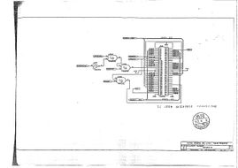
File:Neo Geo Steering Wheel Schematic.jpg|Steering wheel schematic for Thrash Rally. | |||
</gallery> | |||
[[Category:Cartridge systems]] | [[Category:Cartridge systems]] | ||
Latest revision as of 23:58, 24 September 2023
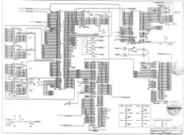
AES (home)
Big thanks to Wolfsoft and ArcadeTV for the scans.
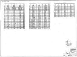
On page 6: There are two resistors in the bottom left corner that can't be seen due the page fold.
The R48 4.7k is connected to VCC and R49 4.7k is connected to GND.
Both resistors are connected to pin3 of U31A.
-
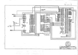
Page 1:68k 68k user RAM NEO-C1
-
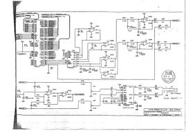
Page 2:NEO-G0 Palette RAM Video DAC
-
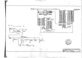
Page 3:NEO-B1 Reset generator Joypad ports
-
-
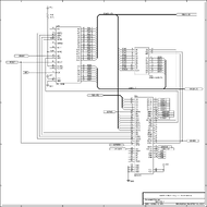
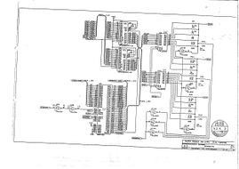
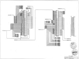
Page 5:Z80 Z80 RAM NEO-D0 (original scan)
-
-
Page 7:Video encoder
-
Page 8:cartridge slot
-
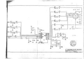
Page 9:System latch NEO-E0 Power supply
-
Page 10:Memory card
-
Page 11:Video PLL


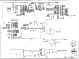
MVS (MV1F)
Beware ! There's an error on page 9 (cartridge edge connections): ROMOE/4MB are swapped. ROMOE should be on pin 33 bottom, and 4MB is on pin 34 bottom.
-
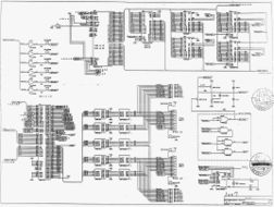
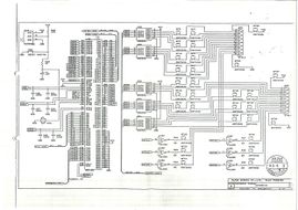
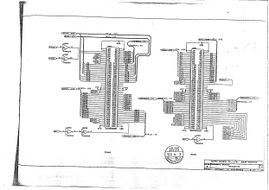
Page 1:68k System ROM 68k user RAM Battery-backed RAM NEO-C1 Joypad ports UPD4990 Battery circuit
-
-
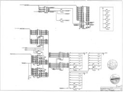
Page 3:NEO-E0 System latch Palette RAM Video DAC
-
-

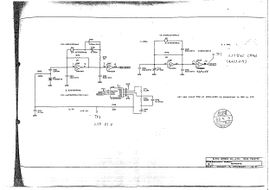
Page 5:Power amp NEO-F0 DIP switches Cab interface
-
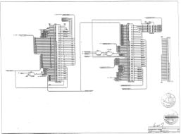
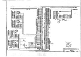
Page 6:Daughterboard connections
-
Page 7
-
Page 8:Daughterboard connections
-
Page 9:Cartridge connections


Peripheral (home/arcade)
-
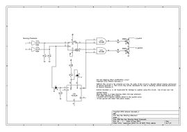
Steering wheel schematic for Thrash Rally.
