Category:Chips: Difference between revisions
Jump to navigation
Jump to search
m (NEO-SDR thumb) |
(Added NEO-244, NEO-253 and manufacturers) |
||
| Line 12: | Line 12: | ||
|- | |- | ||
|[[File:mvs_lspc-a0.jpg|x128px|center]] | |[[File:mvs_lspc-a0.jpg|x128px|center]] | ||
|[[LSPC-A0]] (QFP160) | |[[LSPC-A0]] (NEC QFP160) | ||
|First generation graphics chip | |First generation graphics chip | ||
|Some AES, some MVS | |Some AES, some MVS | ||
| Line 18: | Line 18: | ||
|- | |- | ||
|[[File:aes_lspc2a2.jpg|x128px|center]] | |[[File:aes_lspc2a2.jpg|x128px|center]] | ||
|[[LSPC2-A2]] | |[[LSPC2-A2]] (Fujitsu) | ||
|Second generation graphics chip | |Second generation graphics chip | ||
|Some AES, some MVS | |Some AES, some MVS | ||
| Line 24: | Line 24: | ||
|- | |- | ||
|[[File:Lspc2-a3.jpg|x128px|center]] | |[[File:Lspc2-a3.jpg|x128px|center]] | ||
|[[LSPC2-A3]] | |[[LSPC2-A3]] (Fujitsu) | ||
|Revision of the second generation graphics chip | |Revision of the second generation graphics chip | ||
|Some MVS | |Some MVS | ||
|[[File:Lspc2-a2_pinout.png|x128px|center]] | |[[File:Lspc2-a2_pinout.png|x128px|center]] | ||
|- | |||
|[[File:neo-244.jpg|x128px|center]] | |||
|[[NEO-244]] (Fujitsu QFP64R) | |||
| | |||
|Some MVS | |||
|[[File:neo-244_pinout.png|x128px|center]] | |||
|- | |||
|[[File:neo-253.jpg|x128px|center]] | |||
|[[NEO-253]] (Fujitsu QFP64R) | |||
|Quint 74HC253, 4-to-1 multiplexers | |||
|Some MVS | |||
|[[File:neo-253_pinout.png|x128px|center]] | |||
|- | |- | ||
|[[File:neo-257.jpg|x128px|center]] | |[[File:neo-257.jpg|x128px|center]] | ||
|[[NEO-257]] (QFP64R) | |[[NEO-257]] (Fujitsu QFP64R) | ||
|Quad 74HC257, 2-to-1 multiplexers | |Quad 74HC257, 2-to-1 multiplexers | ||
|Some MVS | |Some MVS | ||
| Line 36: | Line 48: | ||
|- | |- | ||
|[[File:crt_273.jpg|x128px|center]] | |[[File:crt_273.jpg|x128px|center]] | ||
|[[NEO-273]] (QFP64R) | |[[NEO-273]] (Fujitsu QFP64R) | ||
|C and [[S ROM]] address latches | |C and [[S ROM]] address latches | ||
|Cartridges | |Cartridges | ||
| Line 42: | Line 54: | ||
|- | |- | ||
|[[File:aes_b1.jpg|x128px|center]] | |[[File:aes_b1.jpg|x128px|center]] | ||
|[[NEO-B1]] | |[[NEO-B1]] (Fujitsu) | ||
|Second generation graphics chip | |Second generation graphics chip | ||
*Sprite and FIX multiplexer | *Sprite and FIX multiplexer | ||
| Line 51: | Line 63: | ||
|- | |- | ||
|[[File:cd2_buf.jpg|x128px|center]] | |[[File:cd2_buf.jpg|x128px|center]] | ||
|[[NEO-BUF]] | |[[NEO-BUF]] (Fujitsu) | ||
|Dual 8-bit bidirectional buffer | |Dual 8-bit bidirectional buffer | ||
|CD1, CD2, some late MVS | |CD1, CD2, some late MVS | ||
| Line 57: | Line 69: | ||
|- | |- | ||
|[[File:aes_c1.jpg|x128px|center]] | |[[File:aes_c1.jpg|x128px|center]] | ||
|[[NEO-C1]] | |[[NEO-C1]] (Fujitsu) | ||
| | | | ||
*Address decoder | *Address decoder | ||
| Line 66: | Line 78: | ||
|- | |- | ||
|[[File:aes_d0.jpg|x128px|center]] | |[[File:aes_d0.jpg|x128px|center]] | ||
|[[NEO-D0]] (QFP64R) | |[[NEO-D0]] (Fujitsu QFP64R) | ||
|*Audio subsystem controller | |*Audio subsystem controller | ||
*Output port | *Output port | ||
| Line 74: | Line 86: | ||
|- | |- | ||
|[[File:crt_cmc.jpg|x128px|center]] | |[[File:crt_cmc.jpg|x128px|center]] | ||
|[[NEO-CMC]] | |[[NEO-CMC]] (Toshiba) | ||
| | | | ||
*NEO-273 logic | *NEO-273 logic | ||
| Line 87: | Line 99: | ||
|- | |- | ||
|[[File:neo-dcr-t.jpg|x128px|center]] | |[[File:neo-dcr-t.jpg|x128px|center]] | ||
|[[NEO-DCR-T]] | |[[NEO-DCR-T]] (Toshiba) | ||
|? | |? | ||
|Some MVS | |Some MVS | ||
| Line 93: | Line 105: | ||
|- | |- | ||
|[[File:aes_e0.jpg|x128px|center]] | |[[File:aes_e0.jpg|x128px|center]] | ||
|[[NEO-E0]] (QFP64R) | |[[NEO-E0]] (Fujitsu QFP64R) | ||
| | | | ||
*Vector table swapping | *Vector table swapping | ||
| Line 101: | Line 113: | ||
|- | |- | ||
|[[File:mvs_f0.jpg|x128px|center]] | |[[File:mvs_f0.jpg|x128px|center]] | ||
|[[NEO-F0]] (QFP64R) | |[[NEO-F0]] (Fujitsu QFP64R) | ||
| | | | ||
*Calendar access | *Calendar access | ||
| Line 111: | Line 123: | ||
|- | |- | ||
|[[File:aes_g0.jpg|x128px|center]] | |[[File:aes_g0.jpg|x128px|center]] | ||
|[[NEO-G0]] (QFP64R) | |[[NEO-G0]] (Fujitsu QFP64R) | ||
| | | | ||
Quad 245 bidirectional buffer. | Quad 245 bidirectional buffer. | ||
| Line 121: | Line 133: | ||
|- | |- | ||
|[[File:cd2_grc.jpg|x128px|center]] | |[[File:cd2_grc.jpg|x128px|center]] | ||
|[[NEO-GRC]] | |[[NEO-GRC]] (Fujitsu) | ||
|Graphics chip | |Graphics chip | ||
|All CD1, all CD2 | |All CD1, all CD2 | ||
| Line 127: | Line 139: | ||
|- | |- | ||
|[[File:neo-grc2-f.jpg|x128px|center]] | |[[File:neo-grc2-f.jpg|x128px|center]] | ||
|[[NEO-GRC2-F]] | |[[NEO-GRC2-F]] (Fujitsu) | ||
|Graphics chip | |Graphics chip | ||
|All CDZ ?, Some MVS | |All CDZ ?, Some MVS | ||
| Line 133: | Line 145: | ||
|- | |- | ||
|[[File:brd_grz.jpg|x128px|center]] | |[[File:brd_grz.jpg|x128px|center]] | ||
|[[NEO-GRZ]] | |[[NEO-GRZ]] (Fujitsu) | ||
|All-in-one [[GPU]] | |All-in-one [[GPU]] | ||
|ROM-only | |ROM-only | ||
| Line 139: | Line 151: | ||
|- | |- | ||
|[[File:neo-i0.jpg|x128px|center]] | |[[File:neo-i0.jpg|x128px|center]] | ||
|[[NEO-I0]] | |[[NEO-I0]] (Fujitsu) | ||
|Multi-purpose MVS specific chip. | |Multi-purpose MVS specific chip. | ||
*[[SFIX]] ROM address latch | *[[SFIX]] ROM address latch | ||
| Line 147: | Line 159: | ||
|- | |- | ||
|[[File:cd2_mga.jpg|x128px|center]] | |[[File:cd2_mga.jpg|x128px|center]] | ||
|[[NEO-MGA]]<br>NEO-MGA-T<br>NEO-MGA-T2 | |[[NEO-MGA]]<br>NEO-MGA-T<br>NEO-MGA-T2 (Toshiba) | ||
|CD unit interface, latches, address decoding ? | |CD unit interface, latches, address decoding ? | ||
|All CD1, all CD2, all CDZ, some MVS | |All CD1, all CD2, all CDZ, some MVS | ||
| Line 153: | Line 165: | ||
|- | |- | ||
|[[File:cd2_ofc.jpg|x128px|center]] | |[[File:cd2_ofc.jpg|x128px|center]] | ||
|[[NEO-OFC]] | |[[NEO-OFC]] (Fujitsu) | ||
|Graphics chip | |Graphics chip | ||
|All CD1, all CD2 | |All CD1, all CD2 | ||
| Line 159: | Line 171: | ||
|- | |- | ||
|[[File:brd_pcm2.jpg|x128px|center]] | |[[File:brd_pcm2.jpg|x128px|center]] | ||
|[[NEO-PCM2]] | |[[NEO-PCM2]] (Fujitsu) | ||
| | | | ||
*[[PCM]] | *[[PCM]] | ||
| Line 167: | Line 179: | ||
|- | |- | ||
|[[File:neo-sdr-t.jpg|x128px|center]] | |[[File:neo-sdr-t.jpg|x128px|center]] | ||
|[[NEO-SDR-T]] | |[[NEO-SDR-T]] (Toshiba) | ||
|? | |? | ||
|Some MVS, All [[Neo Print]]s | |Some MVS, All [[Neo Print]]s | ||
| Line 173: | Line 185: | ||
|- | |- | ||
|[[File:cd2_sft.jpg|x128px|center]] | |[[File:cd2_sft.jpg|x128px|center]] | ||
|[[NEO-SFT]] | |[[NEO-SFT]] (Fujitsu) | ||
|Graphics related | |Graphics related | ||
|All CD1, all CD2 | |All CD1, all CD2 | ||
| Line 179: | Line 191: | ||
|- | |- | ||
|[[File:cd2_sud.jpg|x128px|center]] | |[[File:cd2_sud.jpg|x128px|center]] | ||
|[[NEO-SUD]] | |[[NEO-SUD]] (Yamaha) | ||
|Z80 subsystem controler | |Z80 subsystem controler | ||
|All CD1, all CD2 | |All CD1, all CD2 | ||
| Line 185: | Line 197: | ||
|- | |- | ||
|[[File:cd2_voc.jpg|x128px|center]] | |[[File:cd2_voc.jpg|x128px|center]] | ||
|[[NEO-VOC]] | |[[NEO-VOC]] (Yamaha) | ||
|PCM memory handler | |PCM memory handler | ||
|All CD1, all CD2 | |All CD1, all CD2 | ||
| Line 191: | Line 203: | ||
|- | |- | ||
|[[File:cd2_ysa.jpg|x128px|center]] | |[[File:cd2_ysa.jpg|x128px|center]] | ||
|[[NEO-YSA]] | |[[NEO-YSA]] (Yamaha) | ||
|Audio subsystem chip | |Audio subsystem chip | ||
|Some CD2 | |Some CD2 | ||
| Line 197: | Line 209: | ||
|- | |- | ||
|[[File:brd_ysa2.jpg|x128px|center]] | |[[File:brd_ysa2.jpg|x128px|center]] | ||
|[[NEO-YSA2]] | |[[NEO-YSA2]] (Yamaha) | ||
|Complete audio subsystem chip | |Complete audio subsystem chip | ||
*Embedded Z80 | *Embedded Z80 | ||
| Line 205: | Line 217: | ||
|- | |- | ||
|[[File:crt_zmc.jpg|x128px|center]] | |[[File:crt_zmc.jpg|x128px|center]] | ||
|[[NEO-ZMC]] (SOIC24) | |[[NEO-ZMC]] (Fujitsu SOIC24) | ||
|Z80 Memory Controller | |Z80 Memory Controller | ||
|Cartridges | |Cartridges | ||
| Line 211: | Line 223: | ||
|- | |- | ||
|[[File:mvs_zmc2.jpg|x128px|center]] | |[[File:mvs_zmc2.jpg|x128px|center]] | ||
|[[NEO-ZMC2]] (QFP80R) | |[[NEO-ZMC2]] (Fujitsu QFP80R) | ||
| | | | ||
*Z80 Memory Controller | *Z80 Memory Controller | ||
| Line 219: | Line 231: | ||
|- | |- | ||
|[[File:crt_pcm.jpg|x128px|center]] | |[[File:crt_pcm.jpg|x128px|center]] | ||
|[[PCM]] (QFP80R) | |[[PCM]] (Fujitsu QFP80R) | ||
| | | | ||
*ADPCM bus latches | *ADPCM bus latches | ||
| Line 234: | Line 246: | ||
|- | |- | ||
|[[File:mvs_pro-b0.jpg|x128px|center]] | |[[File:mvs_pro-b0.jpg|x128px|center]] | ||
|[[PRO-B0]] (QFP136) | |[[PRO-B0]] (NEC QFP136) | ||
|First generation | |First generation | ||
*Palette arbiter | *Palette arbiter | ||
| Line 242: | Line 254: | ||
|- | |- | ||
|[[File:mvs_pro-c0.jpg|x128px|center]] | |[[File:mvs_pro-c0.jpg|x128px|center]] | ||
|[[PRO-C0]] (QFP136) | |[[PRO-C0]] (NEC QFP136) | ||
|First generation | |First generation | ||
*Address decoder | *Address decoder | ||
| Line 252: | Line 264: | ||
|- | |- | ||
|[[File:mvs_pro-ct0.jpg|x64px|center]] | |[[File:mvs_pro-ct0.jpg|x64px|center]] | ||
|[[PRO-CT0]] (SDIP64) | |[[PRO-CT0]] (NEC SDIP64) | ||
|[[C ROM]] character serializer and multiplexer | |[[C ROM]] character serializer and multiplexer | ||
|Some AES carts, some MVS | |Some AES carts, some MVS | ||
| Line 258: | Line 270: | ||
|- | |- | ||
|[[File:brd_pvc.jpg|x128px|center]] | |[[File:brd_pvc.jpg|x128px|center]] | ||
|[[NEO-PVC]] | |[[NEO-PVC]] (Fujitsu) | ||
|[[P ROM]] decryption chip | |[[P ROM]] decryption chip | ||
| | | | ||
| Line 285: | Line 297: | ||
|- | |- | ||
|[[File:aes_68k.jpg|x128px|center]] | |[[File:aes_68k.jpg|x128px|center]] | ||
|[[68k|68HC000]] (DIP64) | |[[68k|68HC000]] (Toshiba DIP64) | ||
|rowspan="2"|16bit CPU | |rowspan="2"|16bit CPU | ||
|All | |All | ||
| Line 294: | Line 306: | ||
|- | |- | ||
|[[File:cd2_68k.jpg|x128px|center]] | |[[File:cd2_68k.jpg|x128px|center]] | ||
|[[68k|68HC000]] (PLCC68) | |[[68k|68HC000]] (Motorola PLCC68) | ||
| | | | ||
|Some | |Some | ||
| Line 319: | Line 331: | ||
|- | |- | ||
|[[File:crt_hd6301.jpg|x128px|center]] | |[[File:crt_hd6301.jpg|x128px|center]] | ||
|[[HD6301]] (DIP40) | |Hitachi [[HD6301]] (DIP40) | ||
|Microcontroller | |Microcontroller | ||
|colspan="5"|[[Multiplayer]] cartridges | |colspan="5"|[[Multiplayer]] cartridges | ||
| Line 360: | Line 372: | ||
|- | |- | ||
|[[File:mvs_upd4990.jpg|x128px|center]] | |[[File:mvs_upd4990.jpg|x128px|center]] | ||
| | |NEC [[UPD4990]] | ||
|Real Time Clock | |Real Time Clock | ||
| | | | ||
| Line 387: | Line 399: | ||
|- | |- | ||
|[[File:aes_z80.jpg|x128px|center]] | |[[File:aes_z80.jpg|x128px|center]] | ||
|[[z80]] (DIP40) | |Zilog [[z80]] (DIP40) | ||
|rowspan="2"|8bit CPU | |rowspan="2"|8bit CPU | ||
|All | |All | ||
| Line 396: | Line 408: | ||
|- | |- | ||
|[[File:cd2_z80.jpg|x128px|center]] | |[[File:cd2_z80.jpg|x128px|center]] | ||
|[[z80]] (SOIC) | |Toshiba [[z80]] (SOIC) | ||
| | | | ||
|Some | |Some | ||
Revision as of 02:02, 16 August 2016
Needed
| Picture | Reference | Description | Found in | Pinout |
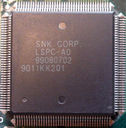 |
LSPC-A0 (NEC QFP160) | First generation graphics chip | Some AES, some MVS | |
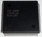 |
LSPC2-A2 (Fujitsu) | Second generation graphics chip | Some AES, some MVS | |
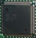 |
LSPC2-A3 (Fujitsu) | Revision of the second generation graphics chip | Some MVS | |
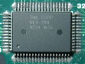 |
NEO-244 (Fujitsu QFP64R) | Some MVS | ||
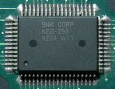 |
NEO-253 (Fujitsu QFP64R) | Quint 74HC253, 4-to-1 multiplexers | Some MVS | 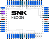 |
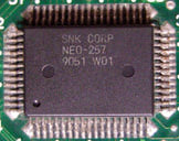 |
NEO-257 (Fujitsu QFP64R) | Quad 74HC257, 2-to-1 multiplexers | Some MVS | 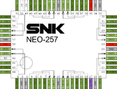 |
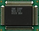 |
NEO-273 (Fujitsu QFP64R) | C and S ROM address latches | Cartridges | |
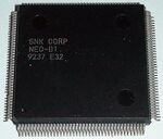 |
NEO-B1 (Fujitsu) | Second generation graphics chip
|
Some AES, some MVS | |
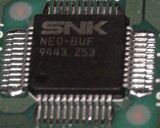 |
NEO-BUF (Fujitsu) | Dual 8-bit bidirectional buffer | CD1, CD2, some late MVS | |
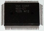 |
NEO-C1 (Fujitsu) |
|
Some AES, some MVS | |
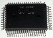 |
NEO-D0 (Fujitsu QFP64R) | *Audio subsystem controller
|
All AES ?, some MVS | |
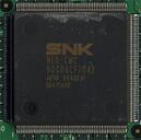 |
NEO-CMC (Toshiba) |
|
Some cartridges | 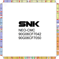 |
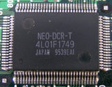 |
NEO-DCR-T (Toshiba) | ? | Some MVS | |
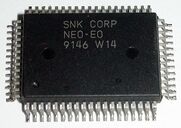 |
NEO-E0 (Fujitsu QFP64R) |
|
Some AES, some MVS | 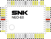 |
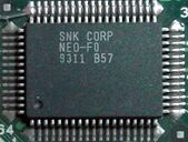 |
NEO-F0 (Fujitsu QFP64R) |
|
Some MVS | |
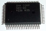 |
NEO-G0 (Fujitsu QFP64R) |
Quad 245 bidirectional buffer.
|
All AES, some MVS ? | |
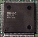 |
NEO-GRC (Fujitsu) | Graphics chip | All CD1, all CD2 | |
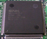 |
NEO-GRC2-F (Fujitsu) | Graphics chip | All CDZ ?, Some MVS | |
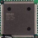 |
NEO-GRZ (Fujitsu) | All-in-one GPU | ROM-only | |
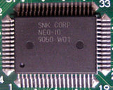 |
NEO-I0 (Fujitsu) | Multi-purpose MVS specific chip.
|
Some MVS | |
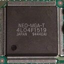 |
NEO-MGA NEO-MGA-T NEO-MGA-T2 (Toshiba) |
CD unit interface, latches, address decoding ? | All CD1, all CD2, all CDZ, some MVS | |
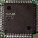 |
NEO-OFC (Fujitsu) | Graphics chip | All CD1, all CD2 | |
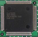 |
NEO-PCM2 (Fujitsu) | ROM-only boards | 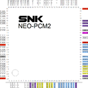 | |
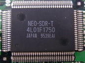 |
NEO-SDR-T (Toshiba) | ? | Some MVS, All Neo Prints | |
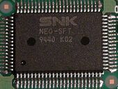 |
NEO-SFT (Fujitsu) | Graphics related | All CD1, all CD2 | |
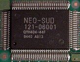 |
NEO-SUD (Yamaha) | Z80 subsystem controler | All CD1, all CD2 | |
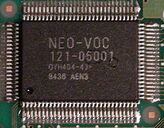 |
NEO-VOC (Yamaha) | PCM memory handler | All CD1, all CD2 | |
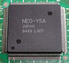 |
NEO-YSA (Yamaha) | Audio subsystem chip | Some CD2 | |
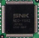 |
NEO-YSA2 (Yamaha) | Complete audio subsystem chip
|
All CDZ ?, All ROM-only | |
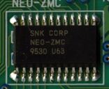 |
NEO-ZMC (Fujitsu SOIC24) | Z80 Memory Controller | Cartridges | |
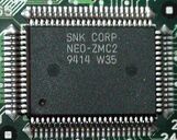 |
NEO-ZMC2 (Fujitsu QFP80R) |
|
AES carts, some MVS | |
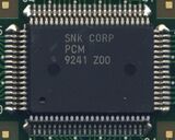 |
PCM (Fujitsu QFP80R) |
|
Cartridges | |
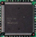 |
PSTG-SNK |
Neo Print GPU. |
||
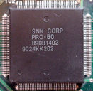 |
PRO-B0 (NEC QFP136) | First generation
|
Some AES, some MVS | |
 |
PRO-C0 (NEC QFP136) | First generation
|
Some AES, some MVS | |
 |
PRO-CT0 (NEC SDIP64) | C ROM character serializer and multiplexer | Some AES carts, some MVS |  |
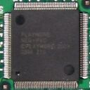 |
NEO-PVC (Fujitsu) | P ROM decryption chip | ||
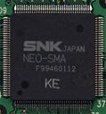 |
NEO-SMA | P ROM decryption chip |
Other chips
| Picture | Reference | Description | Found in | ||||
| AES | MVS | CD1 | CD2 | CDZ | |||
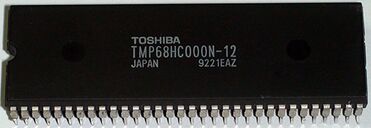 |
68HC000 (Toshiba DIP64) | 16bit CPU | All | Some | |||
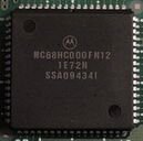 |
68HC000 (Motorola PLCC68) | Some | All | All | All | ||
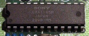 |
Sony CXA1145 | RGB encoder | All | ||||
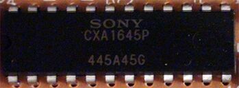 |
Sony CXA1645 | ? | All | ? | |||
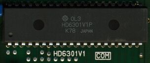 |
Hitachi HD6301 (DIP40) | Microcontroller | Multiplayer cartridges | ||||
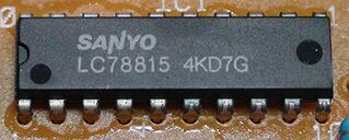 |
Sanyo LC78815 | Stereo DAC | ? | All | |||
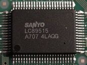 |
Sanyo LC89515 | CD host and error corrector | All | All | ? | ||
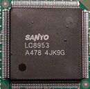 |
Sanyo LC8953 | PUPPET | All | Some | ? | ||
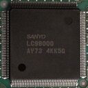 |
Sanyo LC98000 | PUPPET replacement | Some | ? | |||
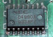 |
NEC UPD4990 | Real Time Clock | All | ||||
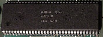 |
Yamaha YM2610 | Sound synthesizer | All | All | All | Some | |
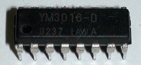 |
Yamaha YM3016 | Audio DAC | All | All | All | Some | |
 |
Zilog z80 (DIP40) | 8bit CPU | All | Some | |||
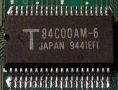 |
Toshiba z80 (SOIC) | Some | All | All | All | ||
Memory chips
| Picture | Reference | Description | Found in |
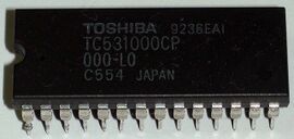 |
LO | Shrink lookup ROM | All systems |
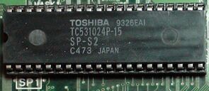 |
SP-S2 | MVS System ROM | MVS systems |
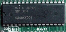 |
SM1 | Embedded sound driver ROM | |
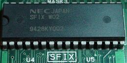 |
SFIX | Embedded Fix ROM | |
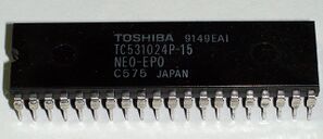 |
NEO-EP0 | AES System ROM | AES systems |
| Picture needed | TOP-SP1-1 | CD2 System ROM | Top loading CD systems (LC8953 versions) |
| Picture needed | TOP-SP1-2 | CD2 System ROM | Top loading CD systems (LC98000 versions) |
| FRONT-SP1 | CD1 System ROM | Front loading CD systems |
Pages in category "Chips"
The following 108 pages are in this category, out of 108 total.
6
C
D
H
L
N
- NEO-244
- NEO-253
- NEO-257
- NEO-273
- NEO-B1
- NEO-BUF
- NEO-C1
- NEO-CDA board
- NEO-CDD board
- NEO-CMC
- NEO-D0
- NEO-DCR-T
- NEO-E0
- NEO-EP0
- NEO-F0
- NEO-FTC1B board
- NEO-G0
- NEO-GRC
- NEO-GRC2
- NEO-GRZ
- NEO-HYCS
- NEO-I0
- NEO-MGA
- NEO-MGA-T
- NEO-OFC
- NEO-PCM2
- NEO-PVC
- NEO-SDR-T
- NEO-SFT
- NEO-SMA
- NEO-SUD
- NEO-VOC
- NEO-YSA
- NEO-YSA2
- NEO-ZMC
- NEO-ZMC2
- NGPC flash board
- NJM2066
